LTC1196 查看數據表(PDF) - Linear Technology
零件编号
产品描述 (功能)
生产厂家
LTC1196 Datasheet PDF : 28 Pages
| |||
LTC1196/LTC1198
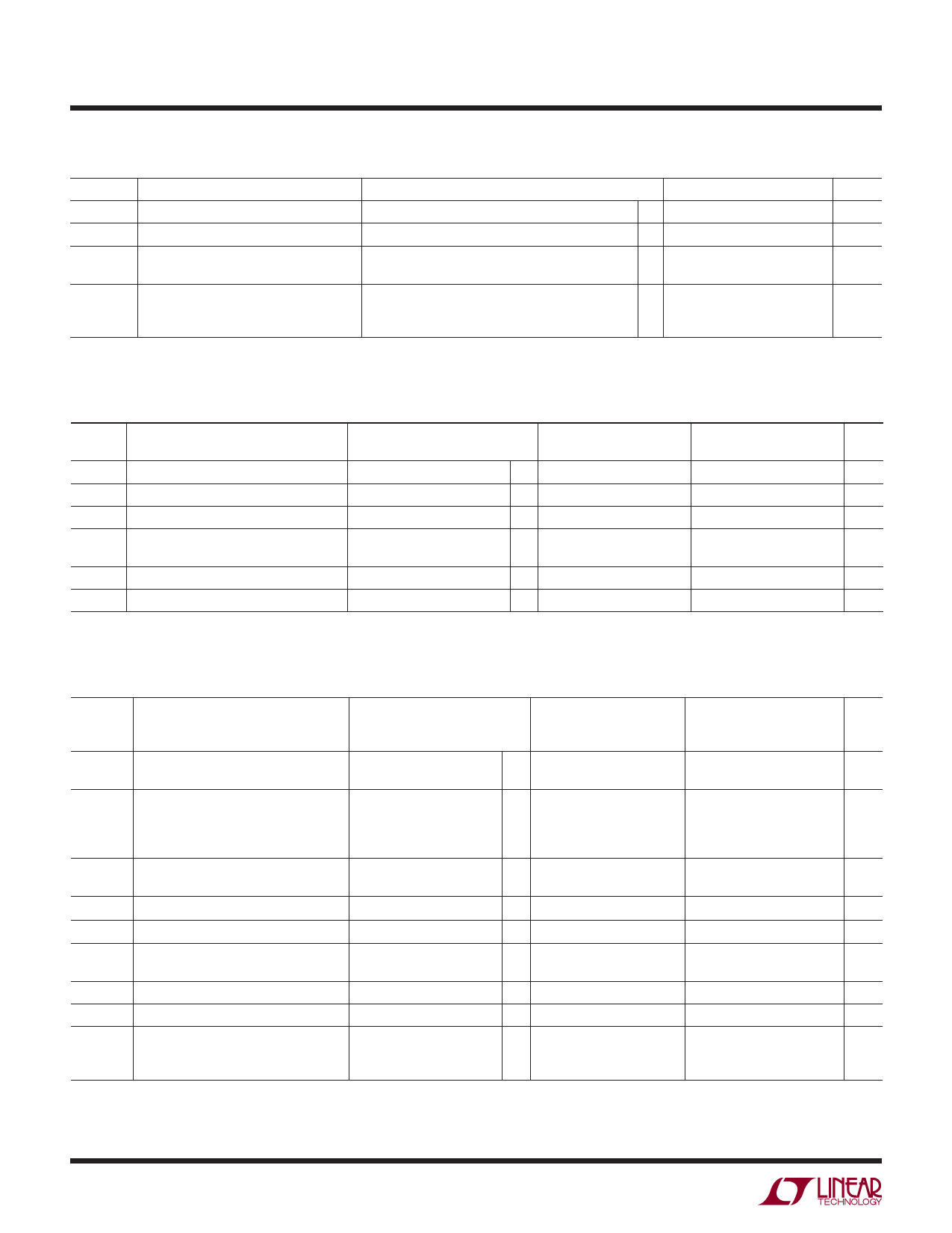
DIGITAL AND DC ELECTRICAL CHARACTERISTICS The l denotes the specifications which apply
over the full operating temperature range, otherwise specifications are at TA = 25°C. VCC = 2.7V, VREF = 2.5V, unless otherwise noted.
SYMBOL PARAMETER
CONDITIONS
MIN TYP MAX UNITS
ISOURCE Output Source Current
VOUT = 0V
–10
mA
ISINK
Output Sink Current
VOUT = VCC
15
mA
IREF
Reference Current, LTC1196
CS = VCC
fSMPL = fSMPL(MAX)
l
0.001 3.0
μA
l
0.25
0.5
mA
ICC
Supply Current
CS
CS
=
=
VCC
VCC
=
=
3.3V,
3.3V,
LTC1198
LTC1196
(Shutdown)
l
l
0.001 3.0
μA
1.5
4.5
mA
fSMPL = fSMPL(MAX), LTC1196/LTC1198
l
2.0
6.0
mA
DYNAMIC ACCURACY The l denotes the specifications which apply over the full operating temperature range,
otherwise specifications are at TA = 25°C. VCC = 2.7V, VREF = 2.5V, fCLK = fCLK(MAX) as defined in Recommended Operating Conditions,
unless otherwise noted.
SYMBOL PARAMETER
CONDITIONS
S/(N + D) Signal-to-Noise Plus Distortion
190kHz/380kHz Input Signal
THD
Total Harmonic Distortion
190kHz/380kHz Input Signal
Peak Harmonic or Spurious Noise
190kHz/380kHz Input Signal
IMD
Intermodulation Distortion
Full-Power Bandwidth
fIN1 = 189.37kHz
fIN2 = 192.446kHz
Full Linear Bandwidth [S/(N + D) > 44dB
LTC1196
MIN TYP MAX
47/45
49/47
53/46
51
LTC1198
MIN TYP MAX UNITS
47/45
dB
49/47
dB
55/46
dB
51
dB
5
5
MHz
0.5
0.5
MHz
AC CHARACTERISTICS The l denotes the specifications which apply over the full operating temperature range,
otherwise specifications are at TA = 25°C. VCC = 2.7V, VREF = 2.5V, fCLK = fCLK(MAX) as defined in Recommended Operating Conditions,
unless otherwise noted.
SYMBOL PARAMETER
tCONV
Conversion Time (See Figures 1, 2)
CONDITIONS
fSMPL(MAX) Maximum Samping Frequency
tdDO
Delay Time, CLK↑ to DOUT Data Valid
LTC1196
LTC1196
LTC1198
LTC1198
CLOAD = 20pF
tDIS
Delay Time CS↑ to DOUT Hi-Z
ten
Delay Time, CLK↓ to DOUT Enabled
CLOAD = 20pF
thDO
Time Output Data Remains Valid After CLOAD = 20pF
CLK↑
tf
DOUT Fall Time
tr
DOUT Rise
CIN
Input Capacitance
CLOAD = 20pF
CLOAD = 20pF
Analog Input On Channel
Analog Input Off Channel
Digital Input
LTC1196-1
LTC1198-1
MIN TYP MAX
LTC1196-2
LTC1198-2
MIN TYP MAX UNITS
1.58
l
1.85
2.13
μs
2.84
μs
450
333
kHz
l 383
250
kHz
337
250
kHz
l 287
187
kHz
100 150
l
180
130
200
ns
250
ns
l
110 220
120
250
ns
l
80
130
100
200
ns
l 45
90
45
120
ns
l
10
30
l
10
30
30
5
5
15
40
ns
15
40
ns
30
pF
5
pF
5
pF
Note 1: Stresses beyond those listed under Absolute Maximum Ratings
may cause permanent damage to the device. Exposure to any Absolute
Maximum Rating condition for extended periods may affect device
reliability and lifetime.
119698fa
6
Share Link: 