PJ7800 查看數據表(PDF) - Unspecified
零件编号
产品描述 (功能)
生产厂家
PJ7800 Datasheet PDF : 9 Pages
| |||
PJ7800 Series
3-Terminal Fixed Voltage Positive Regulators
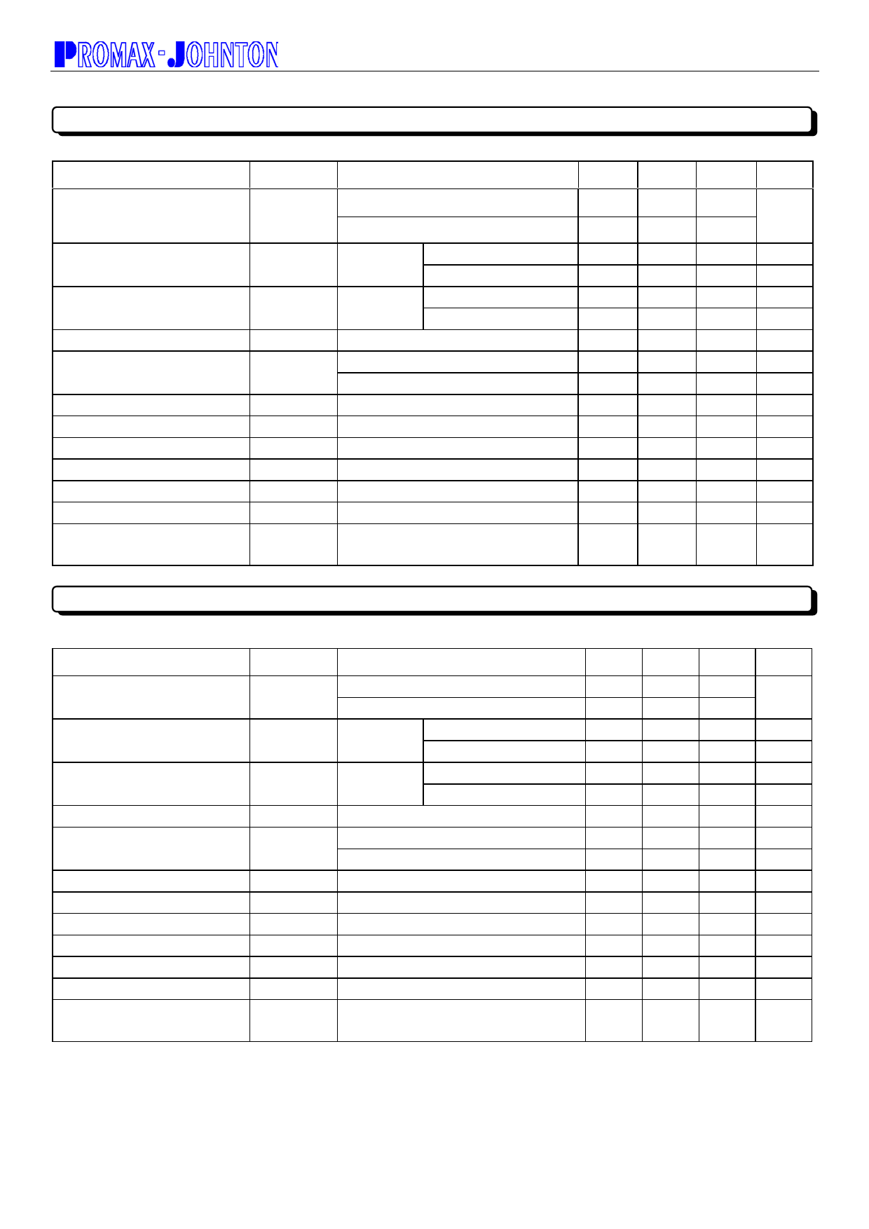
• PJ7806 ELECTRICAL CHARACTERISTICS
(Vin=11V, Iout=500mA, 0℃≤Tj≤125℃, Cin=0.33μF, Cout=0.1μF; unless otherwise specified.)
CHARACTERISTICS
Output Voltage
SYMBOL
Vout
TEST CONDITIONS
Tj=25℃
8V≤Vin≤21V, 5mA≤Iout≤1.5A, PD≤15W
MIN.
5.75
6.3
TYP.
6
6
Line Regulation
Tj=25℃
REGline
8V≤Vin≤25V
9V≤Vin≤13V
--
5
--
1.5
Load Regulation
Tj=25℃ 5mA≤Iout≤1.5A
--
14
REGload
250mA≤Iout≤750mA
--
4
Quiescent Current
Iq
Iout=0, Tj=25℃
--
4.3
Quiescent Current Change
Δlq
8V≤Vin≤25V
5mA≤Iout≤1.5A
--
--
--
--
Output Noise Voltage
Vn
10Hz≤f≤100KHz, Tj=25℃
--
45
Ripple Rejection Ratio
RR
f=120Hz, 9V≤Vin≤19V
59
75
Voltage Drop
Vdrop Iout=1.0A, Tj=25℃
--
2
Output Resistance
Rout
f=1KHz
--
19
Output Short Circuit Current
Ios
Tj=25℃
--
550
Peak Output Current
Io peak Tj=25℃
--
2.2
Temperature Coefficient of
ΔVout/ΔTj Iout=5mA, 0℃≤Tj≤125℃
--
-0.7
Output Voltage
MAX.
6.25
6.3
120
60
120
60
8
1.3
0.5
--
--
--
--
--
--
--
UNIT
V
mV
mV
mV
mV
mA
mA
mA
μV
dB
V
mΩ
mA
A
mV/℃
• PJ7808 ELECTRICAL CHARACTERISTICS
(Vin=14V, Iout=500mA, 0℃≤Tj≤125℃, Cin=0.33μF, Cout=0.1μF; unless otherwise specified.)
CHARACTERISTICS
SYMBOL
TEST CONDITIONS
MIN. TYP. MAX. UNIT
Output Voltage
Tj=25℃
7.69
8
8.32
Vout
V
10.5V≤Vin≤23V, 5mA≤Iout≤1.5A, PD ≤15W 7.61
8
8.40
Line Regulation
REGline Tj=25℃
10.5V≤Vin≤25V
11V≤Vin≤17V
--
6
160 mV
--
2
80 mV
Load Regulation
REGload Tj=25℃
10mA≤Iout≤1.5A
250mA≤Iout≤750mA
--
12
160 mV
--
4
80 mV
Quiescent Current
Iq
Iout=0, Tj=25℃
--
4.3
8
mA
Quiescent Current Change
Δlq
10.5V≤Vin≤25V
5mA≤Iout≤1.5A
--
--
1
mA
--
--
0.5 mA
Output Noise Voltage
Vn
10Hz≤f≤100KHz, Tj=25℃
--
52
--
μV
Ripple Rejection Ratio
RR
f=120Hz, 11V≤Vin≤21V
56
72
--
dB
Voltage Drop
Vdrop Iout=1.0A, Tj=25℃
--
2
--
V
Output Resistance
Rout
f=1KHz
--
16
--
mΩ
Output Short Circuit Current
Ios
Tj=25℃
--
450
--
mA
Peak Output Current
Io peak Tj=25℃
--
2.2
--
A
Temperature Coefficient of
ΔVout/ΔTj Iout=5mA, 0℃≤Tj≤125℃
--
-0.8
-- mV/℃
Output Voltage
* Pulse testing techniques are used to maintain the junction temperature as close to the ambient temperature as possible, and
thermal effects must be taken into account separately.
** This specification applies only for DC power dissipation permitted by absolute maximum ratings.
3-9
2002/10.rev. A
Share Link: 