PLL103-05SC 查看數據表(PDF) - PhaseLink Corporation
零件编号
产品描述 (功能)
生产厂家
PLL103-05SC Datasheet PDF : 4 Pages
| |||
Preliminary PLL103-05
1-to-5 Clock Distribution Buffer
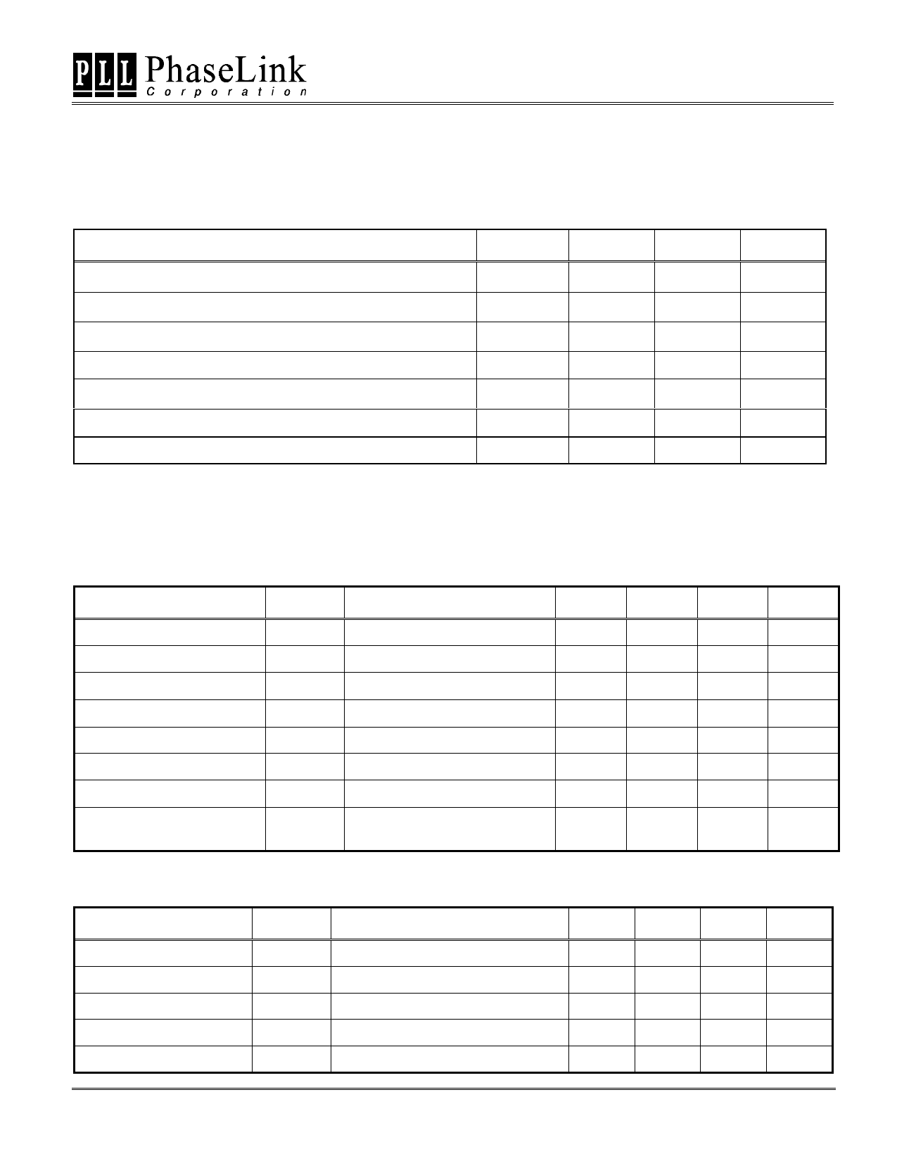
ELECTRICAL SPECIFICATIONS
1. Absolute Maximum Ratings
PARAMETERS
SYMBOL
MIN.
MAX.
UNITS
Supply Voltage Range
Input Voltage Range
Output Voltage Range
Soldering Temperature
Storage Temperature
Ambient Operating Temperature
ESD Voltage
VCC
-0.5
7
V
VI
-0.5
VCC+0.5
V
VO
-0.5
VCC+0.5
V
260
°C
TS
-65
150
°C
0
70
°C
2
kV
Exposure of the device under conditions beyond the limits specified by Maximum Ratings for extended periods may cause permanent damage to the
device and affect product reliability. These conditions represent a stress rating only, and functional operations of the device at these or any other
conditions above the operational limits noted in this specification is not implied.
2. Electrical Characteristics
VDD = 3.0~3.6V, unless otherwise stated
PARAMETERS
SYMBOL
CONDITIONS
Input Low Voltage
Input High Voltage
Input Low Current
Input High Current
Output Low Current
Output High Current
Power Down Supply Current
Supply Current
VIL
VIH
IIL
VIN = 0V
IIH
VIN = VDD
IOL
VOL = 1.5 V
IOH
VOH = 1.5 V
IDD
REF = 0MHz
IDD
Unloaded outputs at 75MHz,
SEL inputs at VDD or GND
MIN.
2.0
TYP.
19
0.10
50
50
0.3
30.0
MAX.
0.8
50.0
100.0
50.0
40.0
UNITS
V
V
µA
µA
mA
mA
µA
mA
3. TIMING CHARACTERISTICS
PARAMETERS
Rise Time
Fall Time
Propagation
Output Duty Cycle
Output-to-Output skew
SYMBOL
CONDITIONS
Tr
Tf
TPROP
DT
Tskew
Measured at 0.8V ~ 2.0V @ 3.3V
Measured at 2.0V ~ 0.8V @ 3.3V
VT = 1.5 V
Rising edges at VDD/2
MIN. TYP. MAX. UNITS
0.8
0.95
1.1
ns
0.78
0.85
0.9
ns
1
4
6
ns
45
50
55
%
250
ps
47745 Fremont Blvd., Fremont, California 94538 TEL (510) 492-0990 FAX (510) 492-0991
Rev 09/26/00 Page 3
Share Link: 