PLL103-06 查看數據表(PDF) - PhaseLink Corporation
零件编号
产品描述 (功能)
生产厂家
PLL103-06 Datasheet PDF : 7 Pages
| |||
Preliminary PLL103-06
DDR SDRAM Buffer with 2 DDR or 3 SDRAM DIMMS
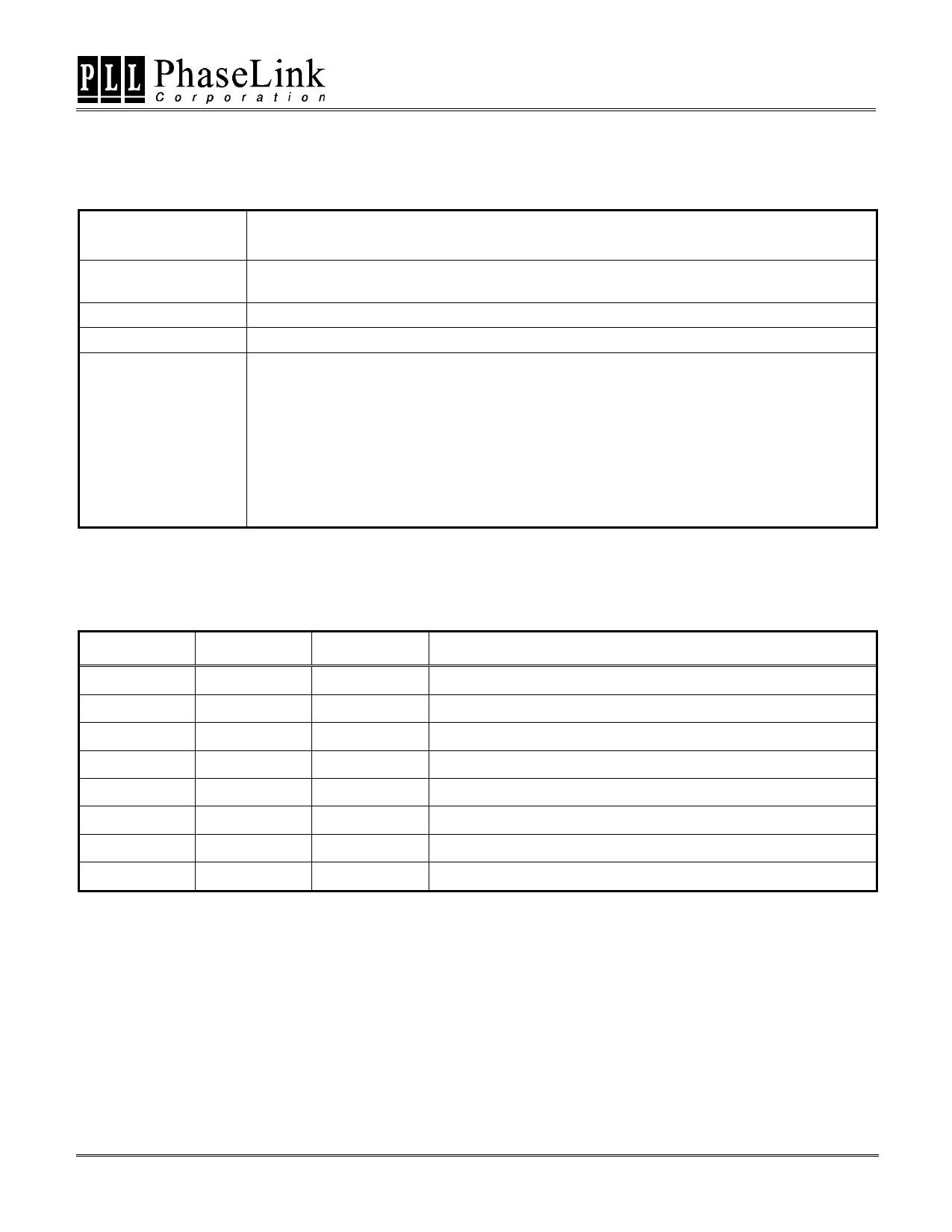
I2C BUS CONFIGURATION SETTING
Address Assignment
A6
1
A5
1
A4
0
A3
1
A2
0
A1
0
A0
1
R/W
_
Slave
Receiver/Transmitter
Provides both slave write and readback functionality
Data Transfer Rate Standard mode at 100kbits/s
Data Protocol
This serial protocol is designed to allow both blocks write and read from the controller. The
bytes must be accessed in sequential order from lowest to highest byte. Each byte transferred
must be followed by 1 acknowledge bit. A byte transferred without acknowledged bit will
terminate the transfer. The write or read block both begins with the master sending a slave
address and a write condition (0xD2) or a read condition (0xD3).
Following the acknowledge of this address byte, in Write Mode: the Command Byte and Byte
Count Byte must be sent by the master but ignored by the slave, in Read Mode: the Byte
Count Byte will be read by the master then all other Data Byte. Byte Count Byte default at
power-up is = (0x09).
I2C CONTROL REGISTERS
1. BYTE 6: Outputs Register (1=Enable, 0=Disable)
Bit
Pin#
Default Description
Bit 7
28
1
SEL_DDR ( I2C is ready only, value is set through pin28 )
Bit 6
-
0
Reserved
Bit 5
-
0
Reserved
Bit 4
1
1
FBOUT
Bit 3
27, 26
1
DDR5T_SDRAM10, DDR5C_SDRAM11
Bit 2
-
1
Reserved
Bit 1
23, 22
1
DDR4T_SDRAM8, DDR4C_SDRAM9
Bit 0
-
1
Reserved
47745 Fremont Blvd., Fremont, California 94538 TEL (510) 492-0990 FAX (510) 492-0991
Rev 12/20/00 Page 3
Share Link: 