PLUS173DN жҹҘзңӢж•ёж“ҡиЎЁпјҲPDFпјү - Philips Electronics
йӣ¶д»¶зј–еҸ·
дә§е“ҒжҸҸиҝ° (еҠҹиғҪ)
з”ҹдә§еҺӮ家
PLUS173DN Datasheet PDF : 8 Pages
| |||
Philips Semiconductors Programmable Logic Devices
Programmable logic arrays
(22 Г— 42 Г— 10)
Product specification
PLUS173B/D
AC ELECTRICAL CHARACTERISTICS
0В°C вүӨ Tamb вүӨ +75В°C, 4.75 вүӨ VCC вүӨ 5.25V, R1 = 300в„Ұ, R2 = 390в„Ұ
LIMITS
SYMBOL
PARAMETER
FROM
TO
TEST
PLUS173B
PLUS173D
UNIT
CONDITION MIN TYP MAX MIN TYP MAX
tPD
Propagation Delay2 Input +/вҖ“ Output +/вҖ“ CL = 30pF
11
15
10
12
ns
tOE
Output Enable1
Input +/вҖ“ Output вҖ“ CL = 30pF
11
15
10
12
ns
tOD
Output Disable1
Input +/вҖ“
Output +
CL = 5pF
11
15
10
12
ns
NOTES:
1. For 3-State outputs; output enable times are tested with CL = 30pF to the 1.5V level, and S1 is open for high-impedance to High tests and
closed for high-impedance to Low tests. Output disable times are tested with CL = 5pF. High-to-High impedance tests are made to an output
voltage of VT = (VOH вҖ“ 0.5V) with S1 open, and Low-to-High impedance tests are made to the VT = (VOL + 0.5V) level with S1 closed.
2. All propagation delays are measured and specified under worst case conditions.
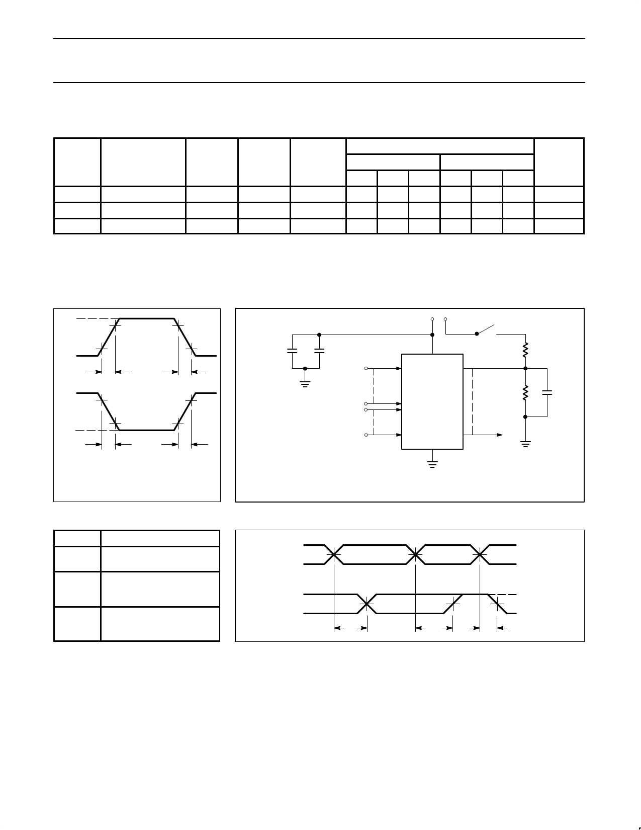
VOLTAGE WAVEFORM
+3.0V
90%
TEST LOAD CIRCUIT
VCC
+5V
S1
0V
+3.0V
10%
5ns
tR tF
5ns
90%
0V
5ns
10%
5ns
MEASUREMENTS:
All circuit delays are measured at the +1.5V level
of inputs and outputs, unless otherwise specified.
Input Pulses
C1
C2
In
BZ
INPUTS
In
DUT
BM
R1
R2
CL
BM GND BZ
OUTPUTS
NOTE:
C1 and C2 are to bypass VCC to GND.
Test Load Circuit
TIMING DEFINITIONS
SYMBOL
PARAMETER
tPD
Propagation delay between
input and output.
tOD
Delay between input change
and when output is off (Hi-Z
or High).
tOE
Delay between input change
and when output reflects
specified output level.
TIMING DIAGRAM
I, B
1.5V
B
1.5V
tPD
1.5V
+3V
1.5V
0V
VOH
VT
1.5V
VOL
tOD
tOE
October 22, 1993
37
Share Link: 