PT6963 查看數據表(PDF) - Princeton Technology
零件编号
产品描述 (功能)
生产厂家
PT6963 Datasheet PDF : 17 Pages
| |||
PT6963
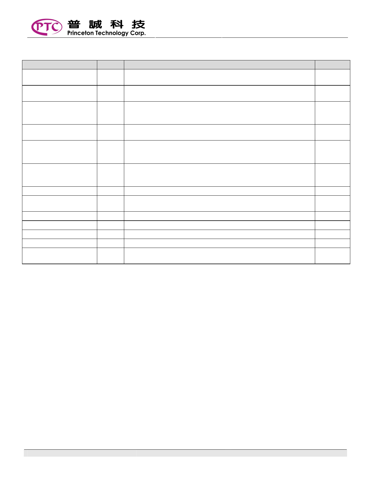
PIN DESCRIPTION
Pin Name
I/O
Description
Pin No.
OSC
I
Oscillator Input Pin
A resistor is connected to this pin to determine the oscillation frequency
1
DOUT
O
Data Output Pin (N-Channel, Open-Drain)
This pin outputs serial data at the falling edge of the shift clock.
2
Data Input Pin
DIN
I This pin inputs serial data at the rising edge of the shift clock (starting
3
from the lower bit)
CLK
I
Clock Input Pin This pin reads serial data at the rising edge and
outputs data at the falling edge.
4
Serial Interface Strobe Pin
STB
I The data input after the STB has fallen is processed as a command.
5
When this pin is “HIGH", CLK is ignored.
K1 ~ K3
Key Data Input Pins
I The data sent to these pins are latched at the end of the display
cycle. (Internal Pull-Low Resistor)
6, 7, 8
VDD
- Power Supply
9, 25
SG1/KS1 ~ SG10/KS10
O
Segment Output Pins (p-channel, open drain)
Also acts as the Key Source
10 ~ 12
14 ~ 20
NC
- No Connection
13
SG11
O Segment Output pins (P-Channel, open drain)
21
SG12/GR7 ~ SG14/GR5 O Segment / Grid Output Pins
22, 23, 24
GND
- Ground Pin
26, 29, 32
GR4 ~ GR1
O Grid Output Pins
27, 28,
30, 31
V1.3
4
Share Link: 