RC5052 查看數據表(PDF) - Fairchild Semiconductor
零件编号
产品描述 (功能)
生产厂家
RC5052
Fairchild Semiconductor

RC5052 Datasheet PDF : 18 Pages
| |||
RC5052
PRODUCT SPECIFICATION
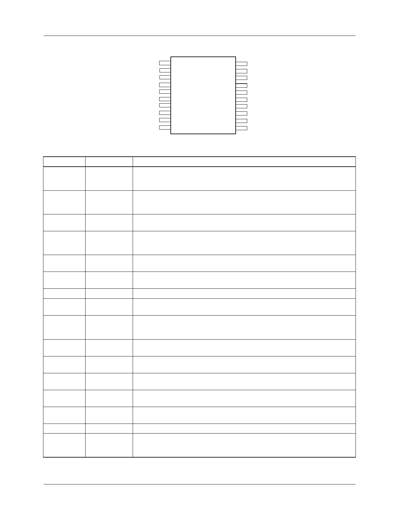
Pin Assignments
ROSC
ENABLE/SS
PWRGD
IFB
VFB
VCCA
OVP
GNDP
LODRV
VCCP
1
20
2
19
3
18
4
RC5052 1 7
5
16
6
15
7
14
8
13
9
12
10
11
VID0
VID1
VID2
VID3
VID4
DTA
GNDA
SW
HIDRV
VCCQP
Pin Definitions
Pin Number
1
Pin Name
ROSC
2
ENABLE/SS
3
PWRGD
4
IFB
5
VFB
6
VCCA
7
OVP
8
GNDP
9
LODRV
10
11
12
13
14
15
16–20
VCCP
VCCQP
HIDRV
SW
GNDA
DTA
VID0-4
Pin Function Description
Oscillator Resistor Connection. Connect an external resistor to this pin to set
the internal oscillator frequency. Layout of this pin is critical to system
performance. See Application Information for details.
Output Enable/Softstart. A logic LOW on this pin will disable the output. An
internal current source allows for open collector control. This pin also doubles as
soft start.
Power Good Flag. An open collector output that will be logic LOW if the output
voltage is not within ±12% of the nominal output voltage setpoint.
Current Feedback. Pin 4 is used in conjunction with pin 13, as the input for the
current feedback control loop. Layout of these traces is critical to system
performance. See Application Information for details.
Voltage Feedback. Pin 5 is used as the input for the voltage feedback control
loop. See Application Information for details regarding correct layout.
Analog VCC. Connect to system 5V supply and decouple with a 0.1µF ceramic
capacitor.
Over Voltage Protection. This pin triggers the gate of an external SCR.
Power Ground. Return pin for high currents flowing in pins 10 and 11. Connect
to a low impedance ground.
Low Side FET Driver. Connect this pin to the gate of an N-channel MOSFET for
synchronous operation. The trace from this pin to the MOSFET gate should be
<0.5".
Power VCC. For low side FET driver. Connect to system 12V supply and
decouple with a 10Ω resistor, 4.7µF tantalum and a 0.1µF ceramic capacitor.
High Side Power VCC. For high side FET driver. Connect to system 12V supply
and decouple with a 10Ω resistor, 4.7µF tantalum and a 0.1µF ceramic capacitor.
High Side FET Driver. Connect this pin to the gate of an N-channel MOSFET.
The trace from this pin to the MOSFET gate should be <0.5".
High side driver source and low side driver drain switching node. Together
with IFB pin allows FET sensing for current.
Analog Ground. Return path for low power analog circuitry. This pin should be
connected to a low impedance system ground plane to minimize ground loops.
Dead Time Adjust. Connect an external resistor to this pin to set the dead time.
Voltage Identification Code Inputs. These open collector/TTL compatible inputs
will program the output voltage over the ranges specified in Table 2. Pull-up
resistors are internal to the controller.
2
REV. 1.3.2 8/27/01
Share Link: