RD74LVC1G98 查看數據表(PDF) - Renesas Electronics
零件编号
产品描述 (功能)
生产厂家
RD74LVC1G98 Datasheet PDF : 10 Pages
| |||
RD74LVC1G98
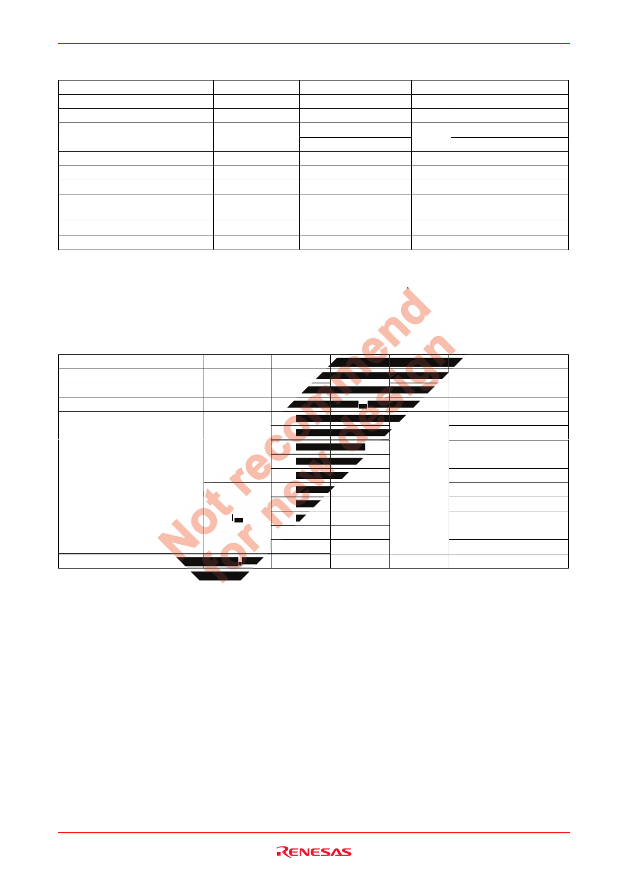
Absolute Maximum Ratings
Item
Symbol
Ratings
Unit
Test Conditions
Supply voltage range
Input voltage range *1
Output voltage range *1, 2
Input clamp current
Output clamp current
Continuous output current
Continuous current through
VCC or GND
Package Thermal impedance
Storage temperature
VCC
VI
VO
IIK
IOK
IO
ICC or IGND
θja
Tstg
–0.5 to 6.5
–0.5 to 6.5
–0.5 to VCC + 0.5
–0.5 to 6.5
–50
–50
±50
±100
123
–65 to 150
V
V
Output : H or L
V
VCC : OFF
mA VI < 0
mA VO < 0
mA VO = 0 to VCC
mA
°C/W WP
°C
Notes:
The absolute maximum ratings are values, which must not individually be exceeded, and furthermore no two
of which may be realized at the same time.
1. The input and output voltage ratings may be exceeded if the input and output clamp-current ratings are
observed.
2. This value is limited to 5.5 V maximum.
Recommended Operating Conditions
Item
Symbol
Min
Supply voltage range
VCC
1.65
Input voltage range
VI
0
Output voltage range
VO
0
—
—
IOL
—
—
—
Output current
—
—
IOH
—
—
—
Operating free-air temperature
Ta
–40
Note: Unused or floating inputs must be held high or low.
Max
5.5
5.5
VCC
4
8
16
24
32
–4
–8
–16
–24
–32
85
Unit
V
V
V
mA
°C
Conditions
VCC = 1.65 V
VCC = 2.3 V
VCC = 3.0 V
VCC = 4.5 V
VCC = 1.65 V
VCC = 2.3 V
VCC = 3.0 V
VCC = 4.5 V
Rev.1.00 Jul 26, 2006 page 5 of 9
Share Link: 