RMPA1852 查看數據表(PDF) - Fairchild Semiconductor
零件编号
产品描述 (功能)
生产厂家
RMPA1852 Datasheet PDF : 11 Pages
| |||
ADVANCED DATA SHEET
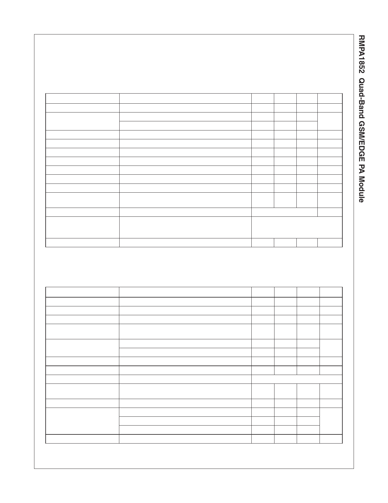
Electrical Specifications
Mode: GMSK Band: CEL Tx band (824–849 MHz)
Modulation: None (CW), Typical Peak/Average = 0dB
Pulse Rate: TX = 577µs, 25% duty cycle, Tframe = 4.615mS
Test conditions unless otherwise stated: Vcc = 3.5V, Vramp = Vramp Max., Zin = Zout = 50Ω, Pin = 3 dBm, Temperature = 25°C,
Duty Cycle = 25%
Parameter
Test Conditions
Frequency
Output Power
Temp = 25°C, Vcc = 3.5 V
Temp = 85°C, Vcc = 2.9 V
Input Power Range
Power Added Efficiency
At Pout max
Input VSWR
Pout = 0 to 35 dBm
Forward Isolation
Pin = 6 dBm
Power Control Range
Vramp = 0.2 to 1.8 V
Harmonics
Cross Band Isolation @ 2fo
Measured at DCS/PCS output.
Stability
Load 6:1, all phase angles, Pin = 3 dBm, Set Vramp
where Pout less than or equal to 34 dBm into a 50Ω load.
Noise Power
Ftx = 824–849, Frx = 869–894 MHz (RBW = 100 KHz)
Ruggedness
VSWR = 10:1, All phase angles, Vcc = 4.8 V, Pin = 3
dBm, Set Vramp where Pout less than or equal to 34.5
dBm into a 50Ω load.
Output Power Switching Speed
RF Pout 5–35 dBm to within 1 dB of final value.
Min
824
34.5
32.5
0
50
–
–
–
–
–
–
–
Typ
–
35
–
+3
55
–
-35
40
–
–
–
Max
849
–
–
+6
–
2.5:1
–
-5
-20
-36
-83
No Damage
–
2
Unit
MHz
dBm
dBm
%
Ratio
dBm
dB
dBm
dBm
dBm
dBm
µS
Mode: EDGE Band: GSM850 Tx band (824–849 MHz)
Modulation: EDGE modulation (3π/8 O-8PSK at 270.833 ksps), Max Peak/Avg = 3.3dB (Probability < 0.1%).
Pulse Rate: TX = 577µs, 25% duty cycle, Tframe = 4.615mS
Input Power: Adjust to meet Output Power Requirement
Parameter
Duty Cycle
Output Power, Pout (H)
Power Added Efficiency
Low power current
consumption mode (L)
Gain
Input VSWR
Harmonics 2Fo Thru 5Fo
Ruggedness
Stability
TX Noise in RX Band
Adjacent Channel Leakage
Error Vector Magnitude
Test Conditions
Max Pi = -0.5 (Temp = 25°C, Vcc = 3.5 V)
at Pout (H), (Temp = 25°C, Vcc = 3.5 V)
Pout<16 dBm
Min
1/8
–
–
at Pout (H)
at Low power current consumption mode (L)
–
At Max Po (Temp = 25°C, Vcc = 3.5 V)
–
VSWR = 10:1, All phase angles, Vcc = 4.8 V, Max Pin = 8
All Spurious (Load VSWR = 6:1 at all angles Po < 29,
–
Pin < 8 dBm)
Ftx = 824–849, Frx = 869–894 MHz (RBW = 100 KHz)
–
Offset : ±200 KHz
–
Offset : ±400 KHz
–
Offset: ±600 KHz
–
Load 50Ω
–
Typ
1/4
29.0
27
Max
1/4
–
–
200
36
25
–
2.0:1
–
-5
No Damage
–
-65
–
-83
–
-33
-57
–
-60
–
4
Unit
dBm
%
mA
dB
Ratio
dBm
dBc
dBm
dBc
%
RMPA1852 Rev. C
3
www.fairchildsemi.com
Share Link: 