RT8061A 查看數據表(PDF) - Richtek Technology
零件编号
产品描述 (功能)
生产厂家
RT8061A Datasheet PDF : 12 Pages
| |||
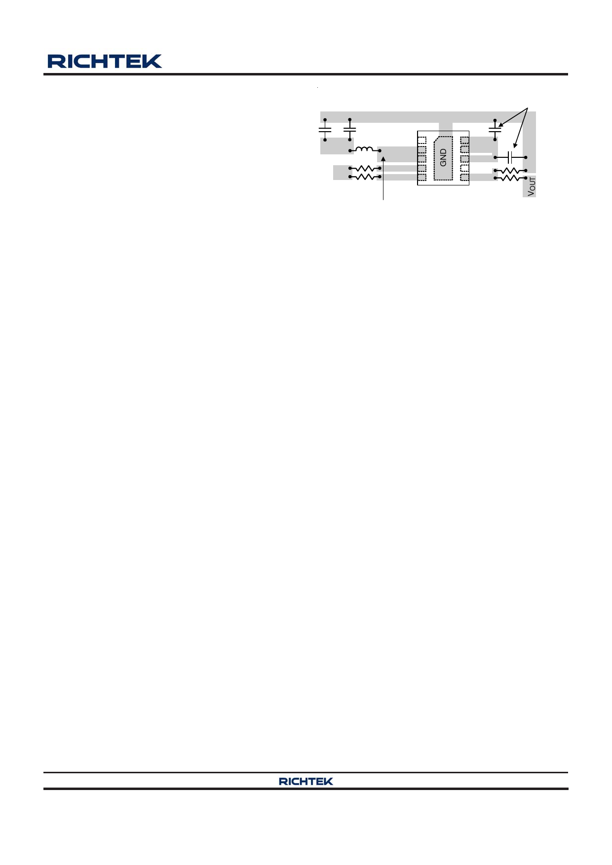
Layout Considerations
Layout is very important in high frequency switching
converter design. The PCB can radiate excessive noise
and contribute to converter instability with improper layout.
Certain points must be considered before starting a layout
using the RT8061A.
` Make the traces of the main current paths as short and
wide as possible.
` Put the input capacitor as close as possible to the device
pins (VIN and GND).
` LX node encounters high frequency voltage swings so
it should be kept in a small area. Keep sensitive
components away from the LX node to prevent stray
capacitive noise pick-up.
` Ensure all feedback network connections are short and
direct. Place the feedback network as close to the chip
as possible.
` The GND pin and Exposed Pad should be connected to
a strong ground plane for heat sinking and noise
protection.
` An example of PCB layout guide is shown in Figure 3.
for reference.
RT8061A
The output capacitor must
be placed near the IC.
COUT
NC 1
VOUT
LX 2
RPGOOD
LX 3
PGOOD 4
VIN
EN 5
REN
Input capacitor must be placed
as close to the IC as possible.
GND
CIN1
10 PVIN
9 PVIN
8 SVIN
7 NC
CIN2
R2
11 6 FB
R1
LX should be connected to inductor by
wide and short trace. Keep sensitive
components away from this trace.
The voltage divider must
be connected as close to
the device as possible.
Figure 3. PCB Layout Guide
Copyright ©2012 Richtek Technology Corporation. All rights reserved.
DS8061A-04 September 2012
is a registered trademark of Richtek Technology Corporation.
www.richtek.com
11
Share Link: 