RT8100 查看數據表(PDF) - Richtek Technology
零件编号
产品描述 (功能)
生产厂家
RT8100 Datasheet PDF : 18 Pages
| |||
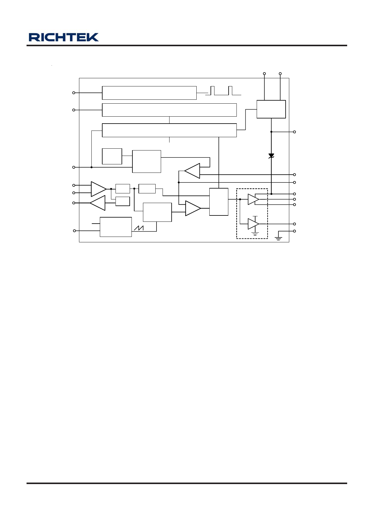
Function Block Diagram
Preliminary
RT8100
12VCC 5VSB
RT
Oscillator free Running 200kHz
SS
Soft Stsrt
CLK
POR Power_sel
EN & VIN Detection
PI
CSN
CSP
I_IND
RR
VREF
+
GM
S/H
-
x4
S/H
CLK
Ramp
Current
Generator
To RR Pin
VREF_SEL
OCP
Current to
Voltage
Converter
+
-
+
-
PWMCP
PWM
Logic
Driver
PVCC
PVCC
FB
COMP
BOOT
UGATE
PHASE
LGATE
GND
Operation
RT8100 is a highly flexible, high performance and high
precision synchronous buck controller specifically
designed for high-end graphic core power supply as well
as DDR applications, with highly reduced external
components and costs.
RT8100 uses RichTek proprietary Analogous Current
ModeTM topology which mimics the traditional peak current
mode by sensing the valley current of the inductor via DCR
sensing techniques and simulating the current ramp with
an artificial ramp set externally. The Analogous Current
Mode topology benefits all the advantages of peak current
mode converter with much higher noise immunity than
conventional one. Since the compensation is easier and
with less constraint than that in voltage mode, using low
ESR output capacitor as MLCC is possible, which therefore
dramatically reduce the board size as well as the cost and
has better transient response due to higher control
bandwidth. RT8100 also adopts VIN feedfoward for ramp
setting, which decreases the complexity for compensation
by keeping the modulator gain constant along line
variations.
The wide input voltage range of the converter ranges from
3.3V to 12V. The output voltage can be set from 0.8V to
3.3V with external resistor divider.
The power sequence of RT8100 includes :
1 : POR function
2 : VIN power supply detection
3 : PI pin setting to enable the whole chip.
The external elements selection of RT8100 includes :
1 : RT pin resister to GND to set the operation frequency
of the chip.
2 : CSN pin resister to set the current gain(ratio of
inductance current IL and sensed current Ix).
3 : RR pin resister to VIN to set the slope of the VIN feed
forward ramp and the effective slope compensation of
current mode.
4 : Use RCSN resister to set the over current level.
5 : Capacitor at SS pin to set the soft-start time.
6 : Type two compensation at COMP pin.
DS8100-03 August 2007
www.richtek.com
5
Share Link: 