RT9515 查看數據表(PDF) - Richtek Technology
零件编号
产品描述 (功能)
生产厂家
RT9515 Datasheet PDF : 11 Pages
| |||
RT9515
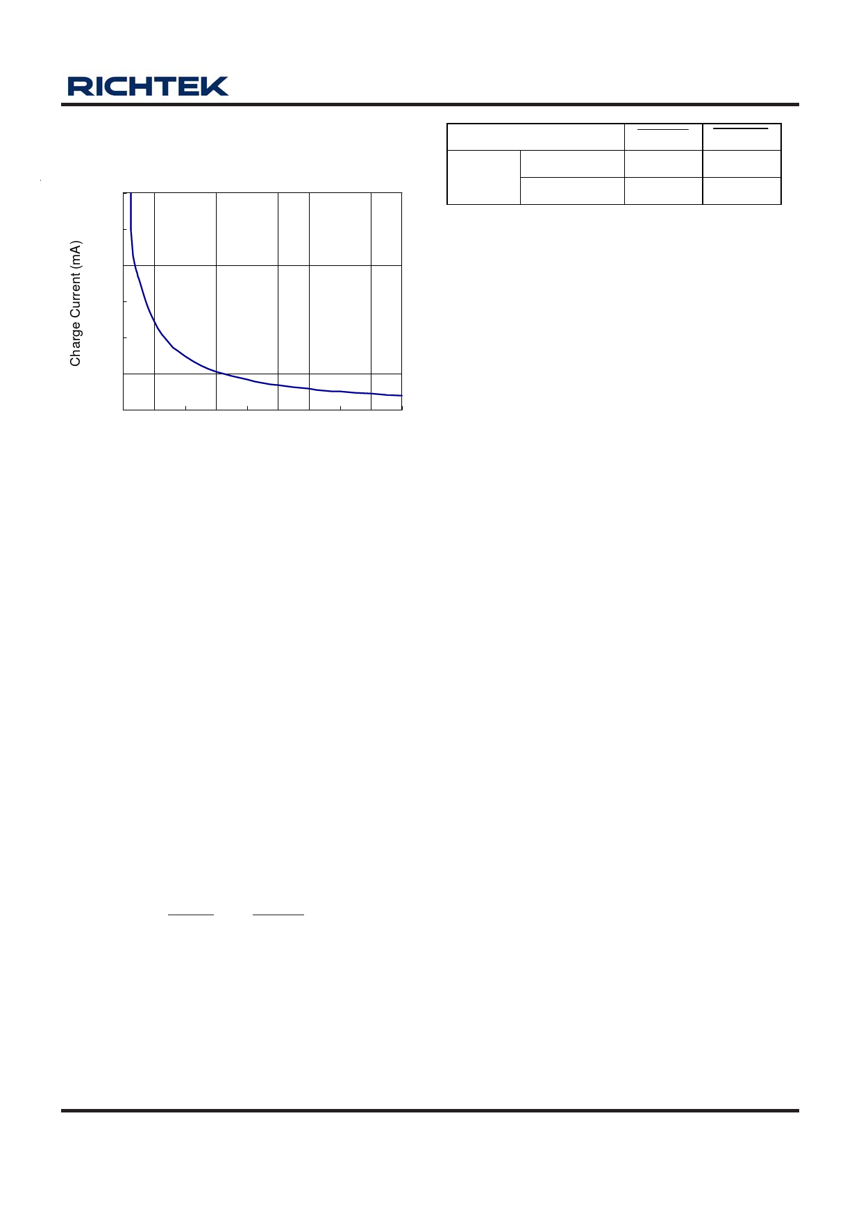
The parameter K = 300 ; VISETA = 2.5V. RSET is the resistor
connected between the ISETA and GND.
1200
1000
800
600
400
200
0
0.5 1.5 2.5 3.5 4.5 5.5 6.5 7.5 8.5 9.5
RSSEETTA(k(Ωk))
Figure 3. Charge Current Setting
Pre- Charge Current Setting
During a charge cycle if the battery voltage is below the
VPRECH threshold, the RT9515 applies a pre-charge mode
to the battery. This feature revives deeply discharged cells
and protects battery life. The RT9515 internally determines
the pre-charge rate as 10% of the fast-charge current.
Battery Voltage Regulation
The RT9515 monitors the battery voltage through the BATT
pin. Once the battery voltage level closes to the VREG
threshold, the RT9515 voltage enters constant phase and
the charging current begins to taper down. When battery
voltage is over the VREG threshold, the RT9515 will stop
charge and keep to monitor the battery voltage. However,
when the battery voltage decreases 100mV below the
VREG, it will be recharged to keep the battery voltage.
Charge Status Outputs
The open-drain CHG_S and PGOOD outputs indicate
various charger operations as shown in the following table.
These status pins can be used to drive LEDs or
communicate to the host processor. Note that ON
indicates the open-drain transistor is turned on and LED
is bright.
Charge State
ACIN
Ch arge
Charge done
CHG_S
ON
OFF
PGOOD
ON
ON
Temperature Regulation and Thermal Protection
In order to maximize the charge rate, the RT9515 features
a junction temperature regulation loop. If the power
dissipation of the IC results in a junction temperature
greater than the thermal regulation threshold (125°C), the
RT9515 throttles back on the charge current in order to
maintain a junction temperature around the thermal
regulation threshold (125°C). The RT9515 monitors the
junction temperature, TJ, of the die and disconnects the
battery from the input if TJ exceeds 125°C. This operation
continues until junction temperature falls below thermal
regulation threshold (125°C) by the hysteresis level. This
feature prevents the chip from damaging.
Selecting the Input and Output Capacitors
In most applications, the most important is the high-
frequency decoupling capacitor on the input of the RT9515.
A 1uF ceramic capacitor, placed in close proximity to input
pin and GND pin is recommended. In some applications
depending on the power supply characteristics and cable
length, it may be necessary to add an additional 10uF
ceramic capacitor to the input. The RT9515 requires a
small output capacitor for loop stability. A 1uF ceramic
capacitor placed between the BATT pin and GND is typically
sufficient.
Thermal Considerations
For continuous operation, do not exceed absolute
maximum operation junction temperature. The maximum
power dissipation depends on the thermal resistance of
IC package, PCB layout, the rate of surroundings airflow
and temperature difference between junction to ambient.
The maximum power dissipation can be calculated by
following formula :
PD(MAX) = ( TJ(MAX) - TA ) / θJA
Where TJ(MAX) is the maximum operation junction
temperature 125°C, TA is the ambient temperature and the
θJA is the junction to ambient thermal resistance.
DS9515-01 April 2011
www.richtek.com
9
Share Link: 