RTD2010 查看數據表(PDF) - Realtek Semiconductor
零件编号
产品描述 (功能)
生产厂家
RTD2010 Datasheet PDF : 11 Pages
| |||
RTD2010
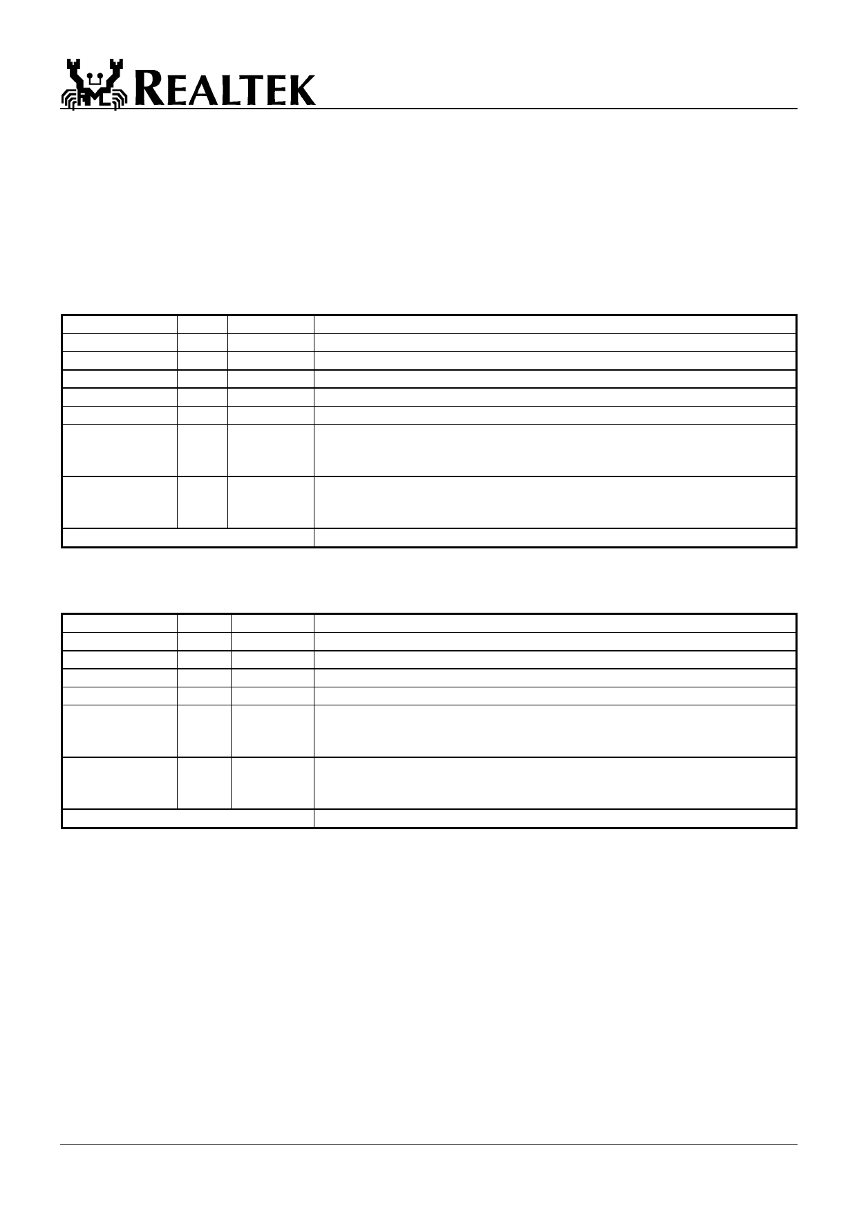
5. Pin Descriptions
In order to reduce pin count, and therefore size and cost, some pins have multiple functions. In those cases, the functions are
separated with a “/” symbol. Refer to the Pin Assignment diagram for a graphical representation.
A = Analog P = Power
I = Input
G = Ground
O = Output
5.1 ADC
Name
ADC_REFIO
ADC_TEST
B
G
R
ADC_VDD
ADC_GND
Type
AI
AIO
AI
AI
AI
AP
AG
Pin No
140
143
146
149
152
141,142
147,148
153,154
138,139
144,145
150,151
Description
ADC Reference Pad
ADC Test Pin / SOG input
Analog Input from BLUE Channel
Analog Input from GREEN Channel
Analog Input from RED Channel
ADC Analog Power
ADC Analog Ground
Total: 17 Pins
5.2 PLL
Name
XI
XO
PLL_TEST1
PLL_TEST2
PLL_VDD
PLL_GND
Type
AI
AO
AIO
AIO
AP
AG
Pin No
92
93
96
97
88,94
95,100
101
89,90
91,98
99,102
Reference Clock Input
Reference Clock Output
Test Pin 1
Test Pin 2
PLL Analog Power
PLL Analog Ground
Description
Total: 15 Pins
2002/11/12
6
Rev1.20
Share Link: 