S-25C080A 查看數據表(PDF) - Seiko Instruments Inc
零件编号
产品描述 (功能)
生产厂家
S-25C080A Datasheet PDF : 39 Pages
| |||
Rev.1.1_00
CMOS SPI 8K SERIAL E2PROM
S-25C080A
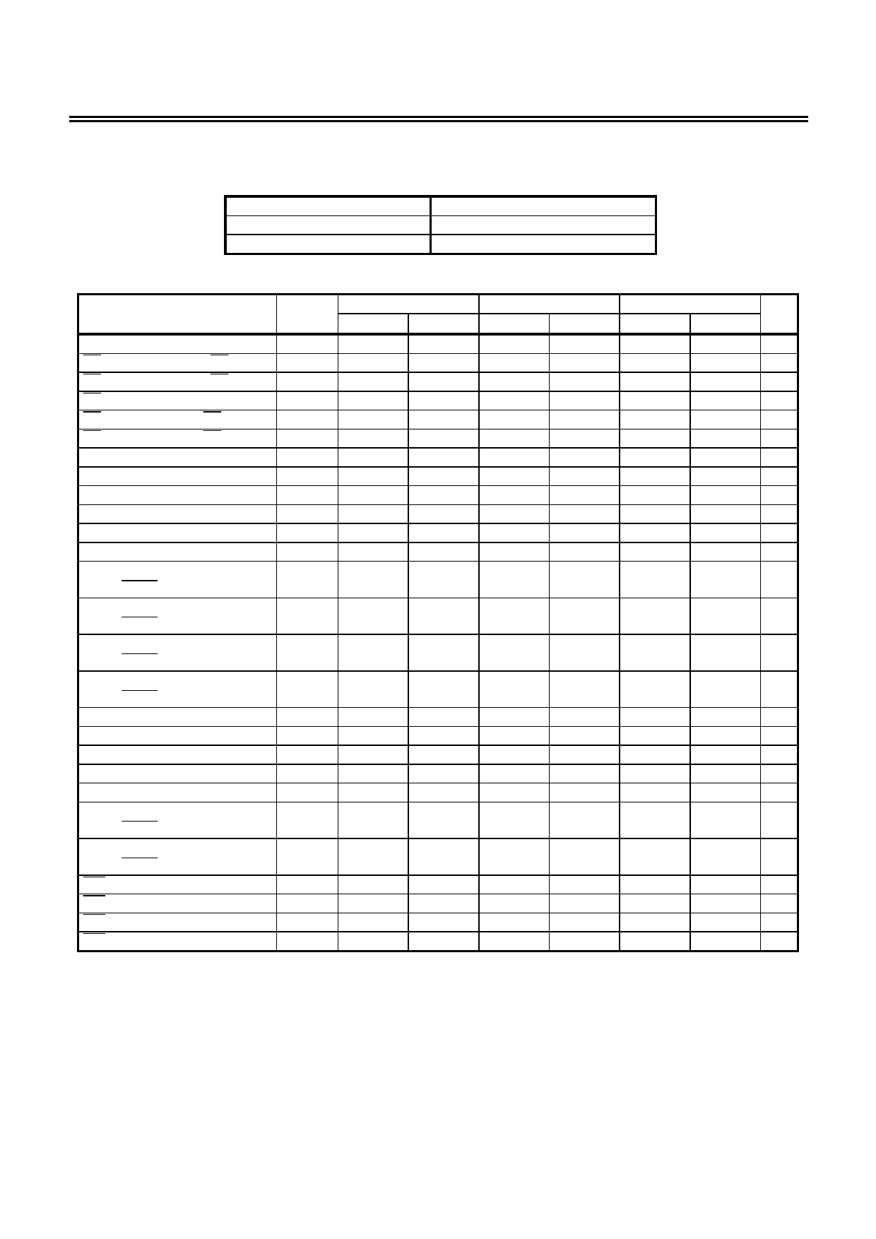
AC Electrical Characteristics
Table 13 Measurement Conditions
Input pulse voltage
Output reference voltage
Output load
0.2 × VCC to 0.8 × VCC
0.5 × VCC
100 pF
Table 14
Item
Symbol VCC = 1.6 to 2.5 V
VCC = 2.5 to 4.5 V
VCC = 4.5 to 5.5 V Unit
Min.
Max.
Min.
Max.
Min.
Max.
SCK clock frequency
fSCK
−
2.0
−
5.0
−
5.0 MHz
CS setup time during CS falling tCSS.CL
150
−
90
−
90
−
ns
CS setup time during CS rising tCSS.CH
150
−
90
−
90
−
ns
CS deselect time
tCDS
200
−
90
−
90
−
ns
CS hold time during CS falling tCSH.CL
200
−
90
−
90
−
ns
CS hold time during CS rising tCSH.CH
150
−
90
−
90
−
ns
SCK clock time “H” *1
tHIGH
200
−
90
−
90
−
ns
SCK clock time “L” *1
tLOW
200
−
90
−
90
−
ns
Rising time of SCK clock *2
tRSK
−
1
−
1
−
1
µs
Falling time of SCK clock *2
tFSK
−
1
−
1
−
1
µs
SI data input setup time
tDS
50
−
20
−
20
−
ns
SI data input hold time
tDH
60
−
30
−
30
−
ns
SCK “L” hold time
during HOLD rising
tSKH.HH
150
−
70
−
70
−
ns
SCL “L” hold time
during HOLD falling
tSKH.HL
100
−
40
−
40
−
ns
SCK “H” setup time
during HOLD falling
tSKS.HL
150
−
60
−
60
−
ns
SCK “H” setup time
during HOLD rising
tSKS.HH
150
−
60
−
60
−
ns
Disable time of SO output *2
tOZ
−
200
−
100
−
100
ns
Delay time of SO output
tOD
−
150
−
70
−
70
ns
Hold time of SO output
tOH
Rising time of SO output *2
tRO
Falling time of SO output *2
tFO
0
−
0
−
0
−
ns
−
100
−
40
−
40
ns
−
100
−
40
−
40
ns
Disable time of SO output
during HOLD falling *2
tOZ.HL
−
200
−
100
−
100
ns
Delay time of SO output
during HOLD rising *2
tOD.HH
−
150
−
50
−
50
ns
WP setup time
tWS1
WP hold time
tWH1
WP release / setup time
tWS2
WP release / hold time
tWH2
0
−
0
−
0
−
ns
0
−
0
−
0
−
ns
0
−
0
−
0
−
ns
60
−
30
−
30
−
ns
*1. The clock cycle of the SCK clock (frequency fSCK) is 1/fSCK µs. This clock cycle is determined by a combination of
several AC characteristics. Note that the clock cycle cannot be set as (1/fSCK) = tLOW (Min.) + tHIGH (Min.) by minimizing
the SCK clock cycle time.
*2. These are values of sample and not 100% tested.
Seiko Instruments Inc.
7
Share Link: 