SA5223 查看數據表(PDF) - Philips Electronics
零件编号
产品描述 (功能)
生产厂家
SA5223 Datasheet PDF : 12 Pages
| |||
Philips Semiconductors
Wide dynamic range AGC transimpedance amplifier(150MHz)
Product specification
SA5223
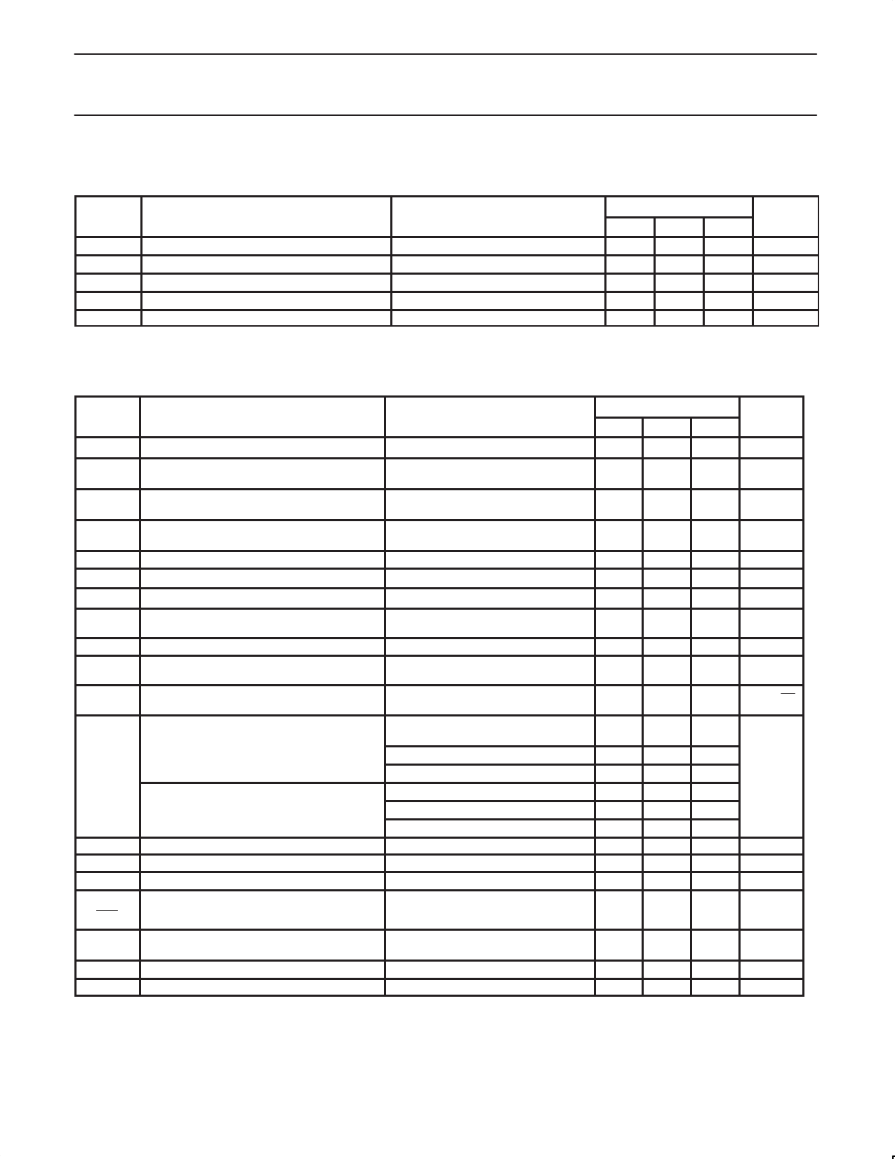
DC ELECTRICAL CHARACTERISTICS
Typical data and Min and Max limits apply at TA = 25°C, and VCC = +5V, unless otherwise specified.
SYMBOL
PARAMETER
TEST CONDITIONS
SA5223
Min Typ Max
VIN
Input bias voltage
1.3
1.55
1.8
VO± Output bias voltage
2.9
3.2
3.5
VOS Output offset voltage (VPIN6 - VPIN7)
-200
80
+200
ICC
Supply current
15
22
29
IOMAX Output sink/source current
1.5
2
NOTE: Standard deviations are estimated from design simulations to represent manufacturing variations over the life of the product.
UNIT
V
V
mV
mA
mA
AC ELECTRICAL CHARACTERISTICS
Typical data and Min and Max limits apply at TA = 25°C and VCC = +5V, unless otherwise specified.
SYMBOL
PARAMETER
TEST CONDITIONS
SA5223
Min Typ Max
UNIT
RT
Transresistance (differential output)
RT
Transresistance
(single-ended output)
DC tested, RL = ∞, IIN = 0-1µA
DC tested, RL = ∞, IIN = 0-1µA
90
125 160
kΩ
45
62.5
80
kΩ
RO
Output resistance
(differential output)
DC tested
140
Ω
RO
f3dB
RIN
CIN
CINT
∆R/∆V
∆R/∆T
IIN
Output resistance
(single-ended output)
Bandwidth (-3dB)
Input resistance
Input capacitance1
Input capacitance including Miller multiplied
capacitance
Transresistance power supply sensitivity
Transresistance ambient temperature sensi-
tivity
RMS noise current spectral density (referred
to input)2
DC tested
Test Circuit 1
DC tested
VCC1 = VCC2 = 5 ±0.5V
∆TA = TA MAX - TA MIN
Test Circuit 2, f = 10MHz
70
110 150
250
0.7
4.0
3
0.09
1.17
Ω
MHz
Ω
pF
pF
%/V
%/oC
pAń ǸHz
Integrated RMS noise current over the band-
width (referred to input)
CS = 0.1pF
IT
CS = 0.4pF
PSRR Power supply rejection ratio (change in VOS)
PSRR Power supply rejection ratio3
Test circuit 2,
∆f = 50MHz
∆f = 100MHz
∆f = 150MHz
∆f = 50MHz
∆f = 100MHz
∆f = 150MHz
DC Tested, ∆VCC = ±0.5V
f = 1.0MHz, Test Circuit 3
7
12
16
nA
8
13
18
–55
dB
–20
dB
VOLMAX Maximum differential output AC voltage
Ii = 0–2mA peak AC
800
mV
dRT
AGC loop time constant parameter4
dt
10µA to 20µA steps
1
dB/ms
IINMAX
Maximum input amplitude for output duty
cycle of 50 ±5%
Test circuit 4
+2
mA
tr, tf Output rise and fall times
10 – 90%
2.2
ns
tD
Group delay
f = 10MHz
2.2
ns
NOTES:
1. Does not include Miller-multiplied capacitance of input device.
2. Noise performance measured differential. Single-ended output noise is higher due to CM noise.
3. PSRR is output referenced and is circuit board layout dependent at higher frequencies. For best performance use a RF filter in VCC line.
4. This implies that the SA5223 gain will change 1dB (10%) in the absence of data for 1ms (i.e., can handle bursty data without degrading Bit
Error Rate (BER) for 100,000 cycles at 100MHz).
1995 Oct 24
3
Share Link: 