SC1545 查看數據表(PDF) - Semtech Corporation
零件编号
产品描述 (功能)
生产厂家
SC1545 Datasheet PDF : 8 Pages
| |||
500mA SmartLDOTM With Power Up
Signal Sequencing
SC1545
PRELIMINARY - January 17, 2000
TIMING DIAGRAMS (Cont.)
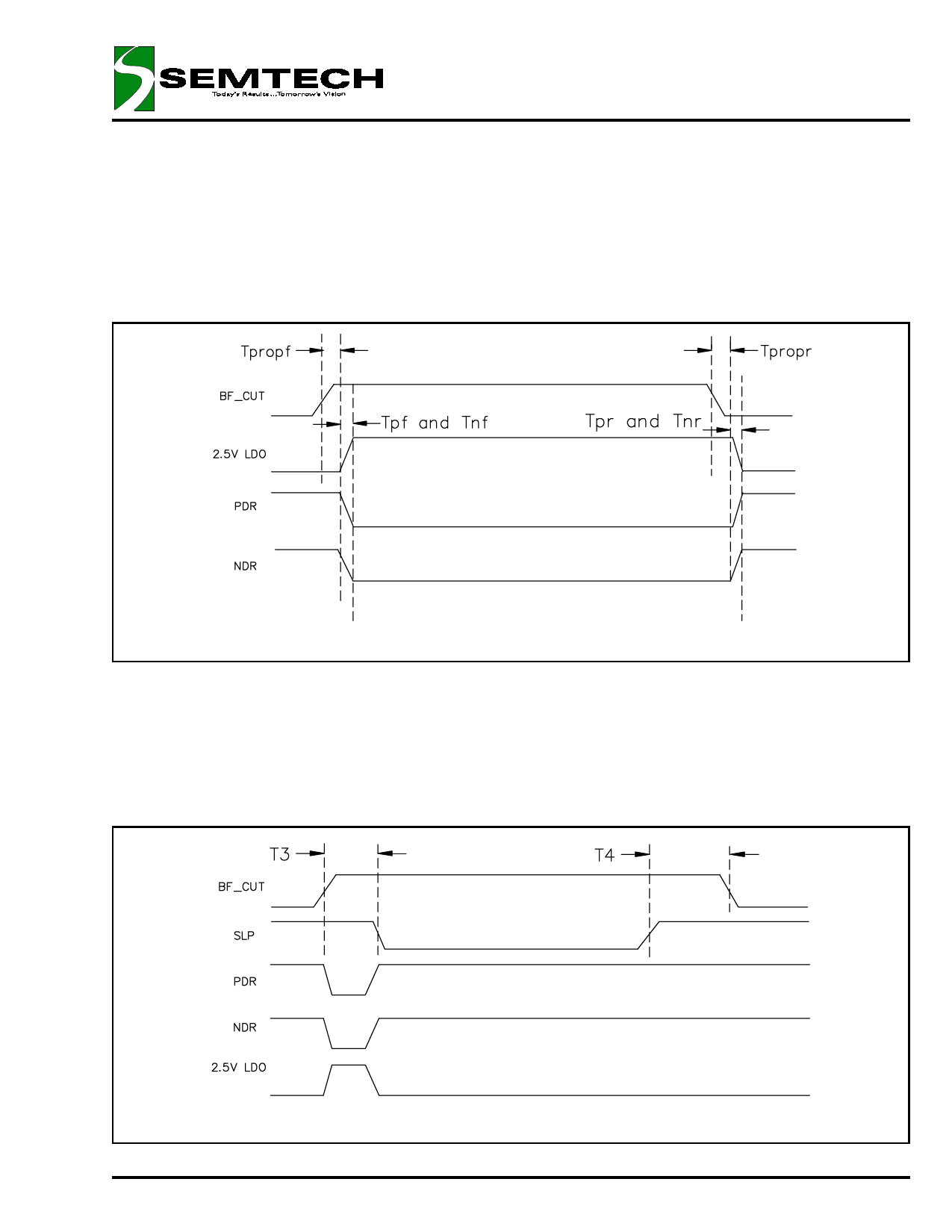
After power up, there are two possible signal sequences that the device will see. The first sequence is with SLP
staying HIGH and BF_CUT transitioning from LOW to HIGH, remaining HIGH for an undetermined period and then
going back to LOW. At this point, the system state is back to where it was at the end of the power up sequence.
The sequence is shown in Figure 2 (below). During these BF_CUT transitions, the propagation delays, rise and fall
times and going into regulation times for PDR, NDR and VO are described in Electrical Characteristics on page 3.
The first sequence can start at any time after the end of the power up sequence.
Figure 2: 1st Sequence Timing
Signal sequencing for the second possible sequence is shown in Figure 3. BF_CUT goes from LOW to HIGH and
SLP goes from HIGH to LOW, 30µsec to 65µsec (T3) later. When BF_CUT goes HIGH, PDR and NDR go LOW
and the 2.5V LDO turns ON. When SLP goes LOW, PDR and NDR return to HIGH and the 2.5V LDO turns OFF.
BF_CUT will stay HIGH and SLP will stay low for an undetermined time, after which SLP will go HIGH. A minimum
of 1msec (T4) later, BF_CUT will go LOW and the system is back at the end of the power up sequence. Typical
measured values of T4 are ~250msec. During all transitions, the propagation delays, rise and fall times, and going
into regulation times for PDR, NDR and 2.5V LDO are described in Electrical Characteristics on page 3. The sec-
ond sequence can start at any time after the end of the power up sequence.
© 2000 SEMTECH CORP.
Figure 3: 2nd Sequence Timing
7
652 MITCHELL ROAD NEWBURY PARK CA 91320
Share Link: 