SC4502H 查看數據表(PDF) - Semtech Corporation
零件编号
产品描述 (功能)
生产厂家
SC4502H Datasheet PDF : 19 Pages
| |||
SC4502/SC4502H
POWER MANAGEMENT
Operation
Applications Information
The SC4502/SC4502H is a programmable constant-
frequency peak current-mode step-up switching regulator
with an integrated power transistor. As shown in the block
diagram in Figure 2, the power transistor is turned on at
the trailing edge of the clock. Switch current is sensed
with an integrated sense resistor. The sensed current
signal is summed with the slope-compensating ramp
before compared to the output of the error amplifier EA.
The PWM comparator trip point determines the switch
turn-on pulse width. The current-limit comparator ILIM
turns off the power switch when the switch current
exceeds the 2A current-limit threshold. ILIM therefore
provides cycle-by-cycle current limit. Current-limit is not
affected by slope compensation because the current limit
comparator ILIM is not in the PWM signal path.
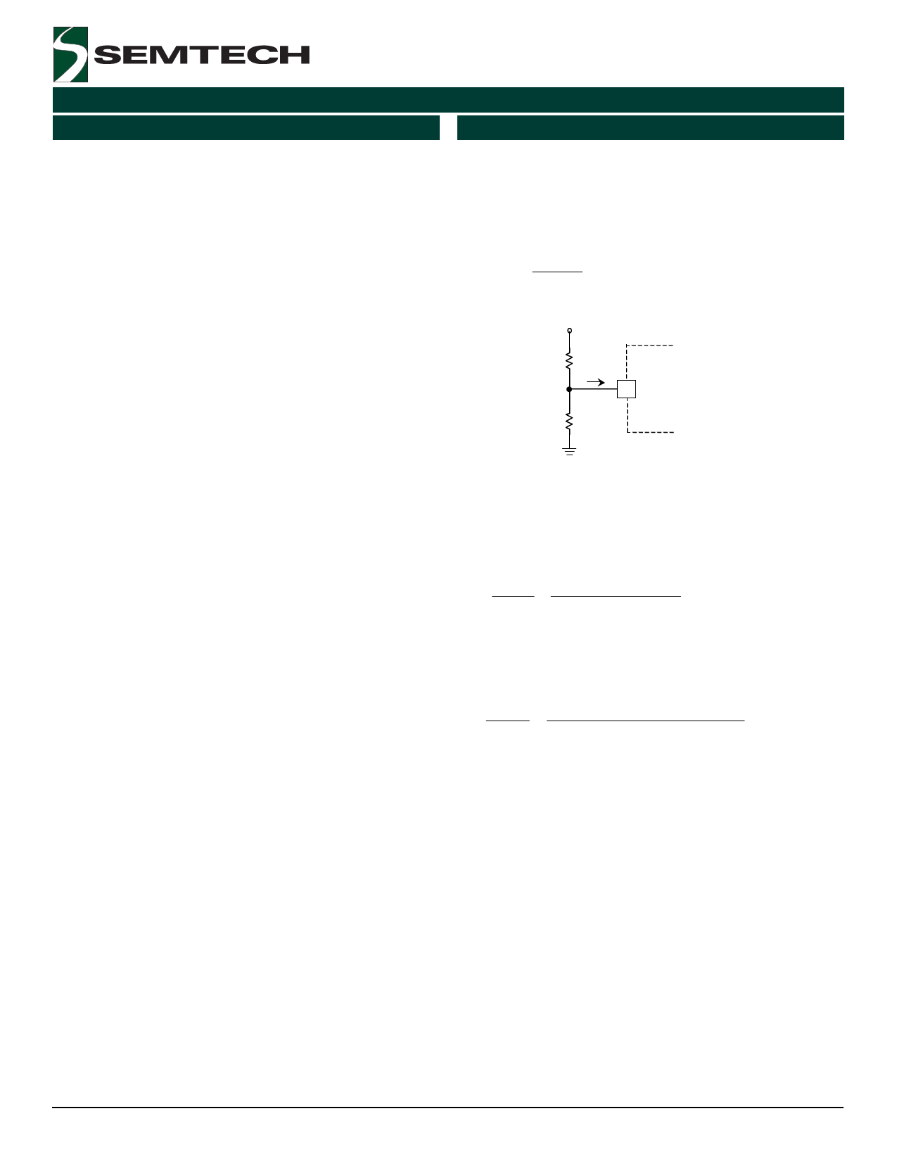
Setting the Output Voltage
An external resistive divider R1 and R2 with its center tap
tied to the FB pin (Figure 3) sets the output voltage.
R1
=
R
2
VOUT
1.242V
− 1
(1)
VOUT
R1
40nA
SC4502/SC4502H
2 FB
R2
Current-mode switching regulators utiilize a dual-loop
feedback control system. In the SC4502/SC4502H the
amplifier output COMP controls the peak inductor current.
This is the inner current loop. The double reactive poles
of the output LC filter are reduced to a single real pole by
the inner current loop, easing loop compensation. Fast
transient response can be obtained with a simple Type-2
compensation network. In the outer loop, the error amplifier
regulates the output voltage.
The switching frequency of the SC4502/SC4502H can
be programmed up to 2MHz with an external resistor
from the ROSC pin to the ground. For converters requiring
extremely low or high duty cycles, the operating frequency
can be lowered to maintain the necessary minimum on
time or the minimum off time.
Figure 3. The Output Voltage is set with a Resistive Divider
The input bias current of the error amplifier will introduce
an error of:
( ) ∆VOUT
VOUT
=
40nA ⋅ R1//R2
1.242V
⋅100 %
(2)
The percentage error of a VOUT = 5V converter with R1 =
100KΩ and R2 = 301KΩ is
∆VOUT
VOUT
=
40nA ⋅ (100KΩ // 301KΩ)⋅100
1.242V
= 0.24%
Operating Frequency and Efficiency
The SC4502/SC4502H requires a minimum input of 1.4V
to operate. A voltage higher than 1.1V at the shutdown
pin enables the internal linear regulator REG in the
SC4502/SC4502H. After VREG becomes valid, the soft-
start capacitor is charged with a 1.5µA current source. A
PNP transistor clamps the output of the error amplifier
as the soft-start capacitor voltage rises. Since the COMP
voltage controls the peak inductor current, the inductor
current is ramped gradually during soft-start, preventing
high input start-up current. Under fault conditions
(VIN<1.4V or over temperature) or when the shutdown
pin is pulled below 1.1V, the soft-start capacitor is
discharged to ground. Pulling the shutdown pin below 0.1V
reduces the total supply current to 10µA.
Switching frequency of SC4502/SC4502H is set with
an external resistor from the ROSC pin to the ground. A
graph showing the relationship between ROSC and
switching frequency is given in the “Typical
Characteristics”.
High frequency operation reduces the size of passive
components but switching losses are higher. The efficiencies
of 5V to 12V converters operating at 700KHz, 1.4MHz
and 2MHz are plotted in Figure 1(b) for SC4502.
Duty Cycle
The duty cycle D of a boost converter in continuous
conduction mode is:
2005 Semtech Corp.
7
www.semtech.com
Share Link: 