SC4502 查看數據表(PDF) - Semtech Corporation
零件编号
产品描述 (功能)
生产厂家
SC4502 Datasheet PDF : 19 Pages
| |||
SC4502/SC4502H
POWER MANAGEMENT
Applications Information
D
=
1−
1−
VIN
VOUT + VD
VCESAT
VOUT + VD
(3)
where VCESAT is the switch saturation voltage and VD is the
voltage drop across the rectifying diode.
It is worth noting that IOUTMAX is directly proportional to the
VIN
ratio of VOUT . Equation (4) over-estimates the maximum
output current at high frequencies (>1MHz) since
switching losses are neglected in its derivation.
Nevertheless it is a useful first-order approximation.
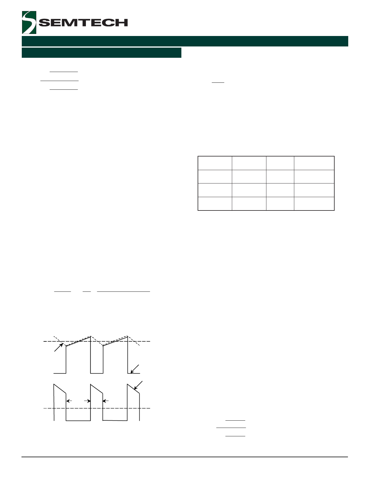
Maximum Output Current
In a boost switching regulator the inductor is connected to
the input. The DC inductor current is the input current.
When the power switch is turned on, the inductor current
flows through the switch. When the power switch is off,
the inductor current flows through the rectifying diode to
the output. The maximum output current is the average
diode current. The diode current waveform is trapezoidal
with pulse width (1 – D)T (Figure 4). The output current
available from a boost converter therefore depends on
the converter operating duty cycle. The power switch
current in the SC4502/SC4502H is internally limited to
2A. This is also the maximum inductor or the input current.
By estimating the conduction losses in both the switch
and the rectifying diode, an expression of the maximum
available output current of a boost converter can be
derived as follows:
( ) IOUTMAX
=
ILIM VIN
VOUT
1−
D
45
−
VD
−D
VD −
VIN
VCESAT
(4)
where ILIM is the switch current limit.
Inductor Current
ON
OFF
ON
IIN
Switch Current
Using VCESAT = 0.3V, VD = 0.5V and ILIM = 1.4A in (3) and
(4), the maximum output currents for three V and V
IN
OUT
combinations are shown in Table 1.
VIN ( V )
2.5
3.3
5
VOUT ( V )
12
5
12
D
0.820
0.423
0.615
IOUTMAX ( A )
0.25
0.80
0.53
Table 1. Calculated Maximum Output Current [ Equation (4)]
Considerations for High Frequency Operation
The operating duty cycle of a boost converter decreases
as VIN approaches VOUT. The PWM modulating ramp in a
current-mode switching regulator is the sensed current
signal. This current ramp is absent unless the switch is
turned on. The intersection of this ramp with the output
of the voltage feedback error amplifier determines the
switch pulse width. The propagation delay time required
to immediately turn off the switch after it is turned on is
the minimum switch on time. Regulator closed-loop
measurement shows that the SC4502/SC4502H has a
minimum on time of about 150ns at room temperature.
The power switch in the SC4502/SC4502H is either not
turned on at all or on for at least 150ns. If the required
switch on time is shorter than the minimum on time, the
regulator will either skip cycles or it will start to jitter.
Diode Current
DT (1-D)T
ON
OFF
ON
OFF
ON
IOUT
Figure 4. Current Waveforms in a Boost Regulator
Example: Determine the maximum operating frequency
of a Li-ion cell to 5V converter using the SC4502.
Assuming that VD=0.5V, VCESAT=0.3V and VIN=2.6V - 4.2V,
the minimum duty ratio can be found using (3).
DMIN
=
1−
1−
4.2
5 + 0.5
0.3
5 + 0.5
= 0.25
2005 Semtech Corp.
8
www.semtech.com
Share Link: 