SCI7661M0A 查看數據表(PDF) - Seiko Epson Corp
零件编号
产品描述 (功能)
生产厂家
SCI7661M0A Datasheet PDF : 9 Pages
| |||
SCI7661COA/MOA
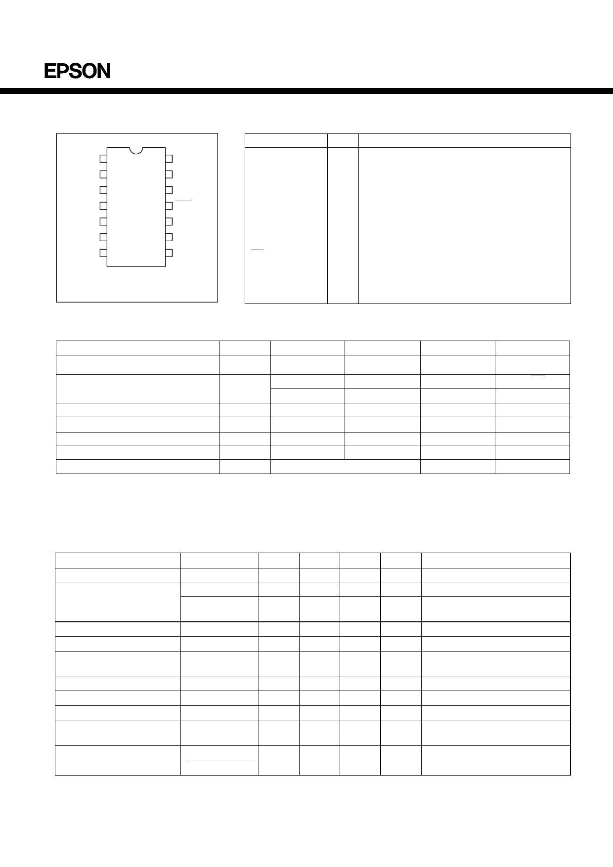
s PIN CONFIGURATION
CAP1+ 1
CAP1- 2
CAP2+ 3
CAP2- 4
TC1
5
TC2
6
VIN
7
14 VDD
13 OSC1
12 OSC2
11 Poff
10 RV
9 Vreg
8 Vout
The same pin configuration in
DIP and SOP
s PIN DESCRIPTION
Pin name
CAP1+, CAP1-
CAP2+, CAP2-
TC1, TC2
VIN
VOUT
Vreg
RV
Poff
OSC2, OSC1
VDD
No.
Function
1, 2 Terminal for connection of capacitor for doubler
3, 4 Terminal for connection of capacitor for tripler
5, 6 Temperature gradient selection terminal
7 Power supply terminal(negative, system supply
GND)
8 Output terminal at tripling
9 Regulated voltage output terminal
10 Regulated voltage control terminal
11 Vreg output ON/OFF control terminal
12, 13 Oscillation resistor connection terminal
14 Power supply terminal(positive system supply
VCC)
s ABSOLUTE MAXIMUM RATINGS
(VDD=0V)
Rating
Input supply voltage
Symbol
VI
Min.
-20/N
Max.
0.5
Unit
V
Remark
NN==23
:
:
Doubler
Tripler
Input terminal voltage
Output voltage
VI
VIN-0.5
0.5
VOUT-0.5
0.5
VO
-20.0
V
OSC1, Poff
V
TC1, TC2, RV
V
Allowable loss
Operating temperature
Storage temperature
Pd
300
mW
Topr
-30
85
°C
Plastic package
Tstg
-55
150
°C
Soldering temperature and time
Tsol
260°C, 10s(at lead)
-
Note: When this IC is soldered in the solder-reflow process, be sure to maintain the reflow furnace at the curve shown in "Fig.
1-5 Reflow Furnace Temperature Curve" of this DATA BOOK. And this IC can not be exposed to high temperature of
the solder dipping.
s ELECTRICAL CHARACTERISTICS
Characteristic
Input supply voltage
Output voltage
Regulator operating voltage
Booster current consumption
Regulator current
consumption
Stationary current
Oscillation frequency
Output impedance
Booster power conversion
efficiency
Regulated output voltage
fluctuation
Symbol
VI
VO
Vreg
VOUT
Iopr1
Iopr2
IQ
fosc
ROUT
Peff
∆Vreg
∆VOUT•Vreg
Min. Typ.
-6.0
-18.0
-18
-18.0
60
50
16
20
150
90
95
0.2
Max.
-1.2
-2.6
-3.2
100
12.0
2.0
24
200
(VDD = 0V, VIN=-5V, Ta=-30 to 85°C)
Unit
Condition
V
V
V
RL=∞, RRV=1MΩ,
VO=-18V
V
µA RL=∞, ROSC=1MΩ
µA
RL=∞, RRV=1MΩ
VOUT=-15V
µA TC2=TC1=VOUT, RL=∞
kHz ROSC=1MΩ
Ω IOUT=10mA
%
IOUT=5mA
%/V
-18V<VOUT<-8V,
Vreg=-8V, RL=∞, Ta=25°C
2
Share Link: 