SG3503 查看數據表(PDF) - Microsemi Corporation
零件编号
产品描述 (功能)
生产厂家
SG3503 Datasheet PDF : 3 Pages
| |||
SG1503/SG2503/SG3503
ABSOLUTE MAXIMUM RATINGS (Note 1)
Input Voltage ....................................................................... 40V
Storage Temperature Range ............................. -65°C to 150°C
Note 1. Exceeding these ratings could cause damage to the device.
THERMAL DATA
T Package:
Thermal Resistance-Junction to Case, θJC ................... 15°C/W
Thermal Resistance-Junction to Ambient, θJA ............ 120°C/W
Y Package:
Thermal Resistance-Junction to Case, θJC .................. 50°C/W
Thermal Resistance-Junction to Ambient, θJA ........... 130°C/W
M Package:
Thermal Resistance-Junction to Case, θJC ................... 60°C/W
Thermal Resistance-Junction to Ambient, θJA ............. 95°C/W
DM Package:
Thermal Resistance-Junction to Case, θJC .................. 55°C/W
Thermal Resistance-Junction to Ambient, θJA ........... 165°C/W
Operating Junction Temperature
Hermetic (T, Y - Package) ............................................. 150°C
Plastic (M, DM - Package) ............................................ 150°C
Lead Temperature (Soldering, 10 Seconds) .................. 300°C
Pb-free / RoHS Peak Solder Reflow Temp (40 sec. max. exp.)........ 260°C (+0, -5)
Note A.
Junction Temperature Calculation:
T
J
=
T
A
+
(P
D
x
θJA).
Note B. The above numbers for θJC are maximums for the limiting
thermal resistance of the package in a standard mount-
ing configuration. The θJA numbers are meant to be
guidelines for the thermal performance of the device/pc-
board system. All of the above assume no ambient
airflow.
RECOMMENDED OPERATING CONDITIONS (Note 2)
Input Voltage .......................................................... 4.5V to 40V
Note 2. Range over which the device is functional.
Operating Ambient Temperature Range
SG1503 ............................................................ -55°C to 125°C
SG2503 ............................................................. -25°C to 85°C
SG3503 ................................................................ 0°C to 70°C
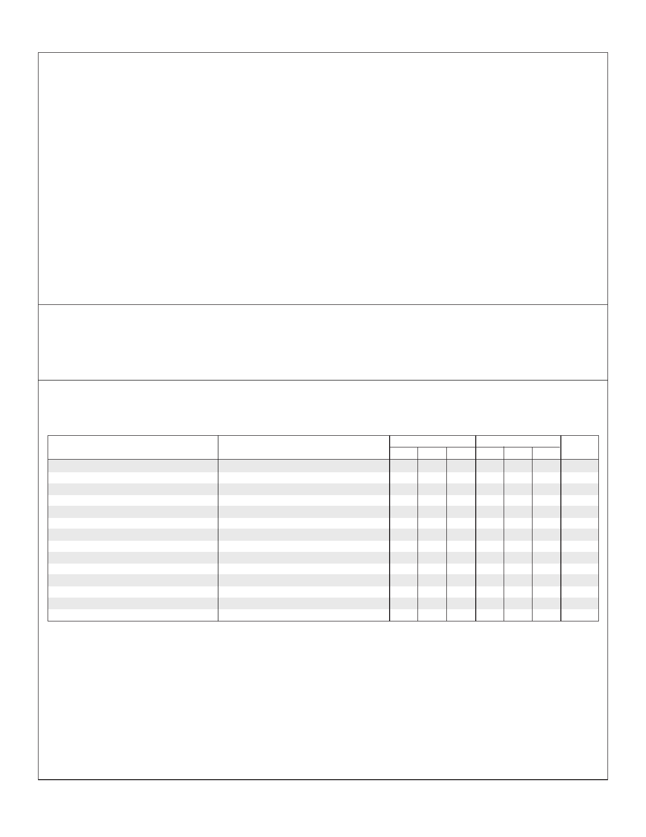
ELECTRICAL CHARACTERISTICS
(Unless
otherwise
specified,
these
specifications
apply
over
the
operating
ambient
temperatures
for
SG1503
with
-55°C
≤
T
A
≤
125°C,
SG2503/SG3503
with 0°C ≤ TA ≤ 70°C, VIN= 15V, and IL = 0mA. Low duty cycle pulse testing techniques are used which maintains junction and case temperatures equal
to the ambient temperature.)
Parameter
Output Voltage
Input Voltage
Line Regulation
Load Regulation
Temperature Regulation
Quiescent Current
Short Circuit Current
Ripple Rejection
Output Noise
Voltage Stability
Test Conditions
TA = 25°C
TA = 25°C
VIN = 5V to 15V
VIN = 15V to 40V
∆IL = 10mA
∆IL = 10mA, VIN = 30V
(SG1503 only)
(SG2503/3503 only)
VIN = 40V
TA = 25°C
f = 120Hz, TA = 25°C
BW
=
10KHz,
T
A
=
25°C
SG1503/2503
SG3503
Min. Typ. Max. Min. Typ. Max.
Units
2.485 2.500 2.515 2.475 2.500 2.525 V
4.7
40 4.7
40
V
4.5
40 4.5
40
V
13
1 3 mV
35
3 10 mV
35
3 10 mV
48
4 15 mV
15 20
mV
2.5 5
5 10 mV
1.5 2.0
1.5 2.0 mA
15 20 30 15 20 30 mA
76
76
dB
100
100
µV rms
250
250
µV/Khr
Rev 1.3a 10/04
Copyright © 1996
Microsemi Inc. - Integrated Products
11861 Western Avenue ∞ Garden Grove, CA 92841
2
(714) 898-8121 ∞ FAX: (714) 893-2570
Share Link: 