SG1844 查看數據表(PDF) - Microsemi Corporation
零件编号
产品描述 (功能)
生产厂家
SG1844 Datasheet PDF : 12 Pages
| |||
PRODUCT DATABOOK 1996/1997
SG1844/SG1845 Series
CURRENT-MODE PWM CONTROLLER
PRODUCTION DATA SHEET
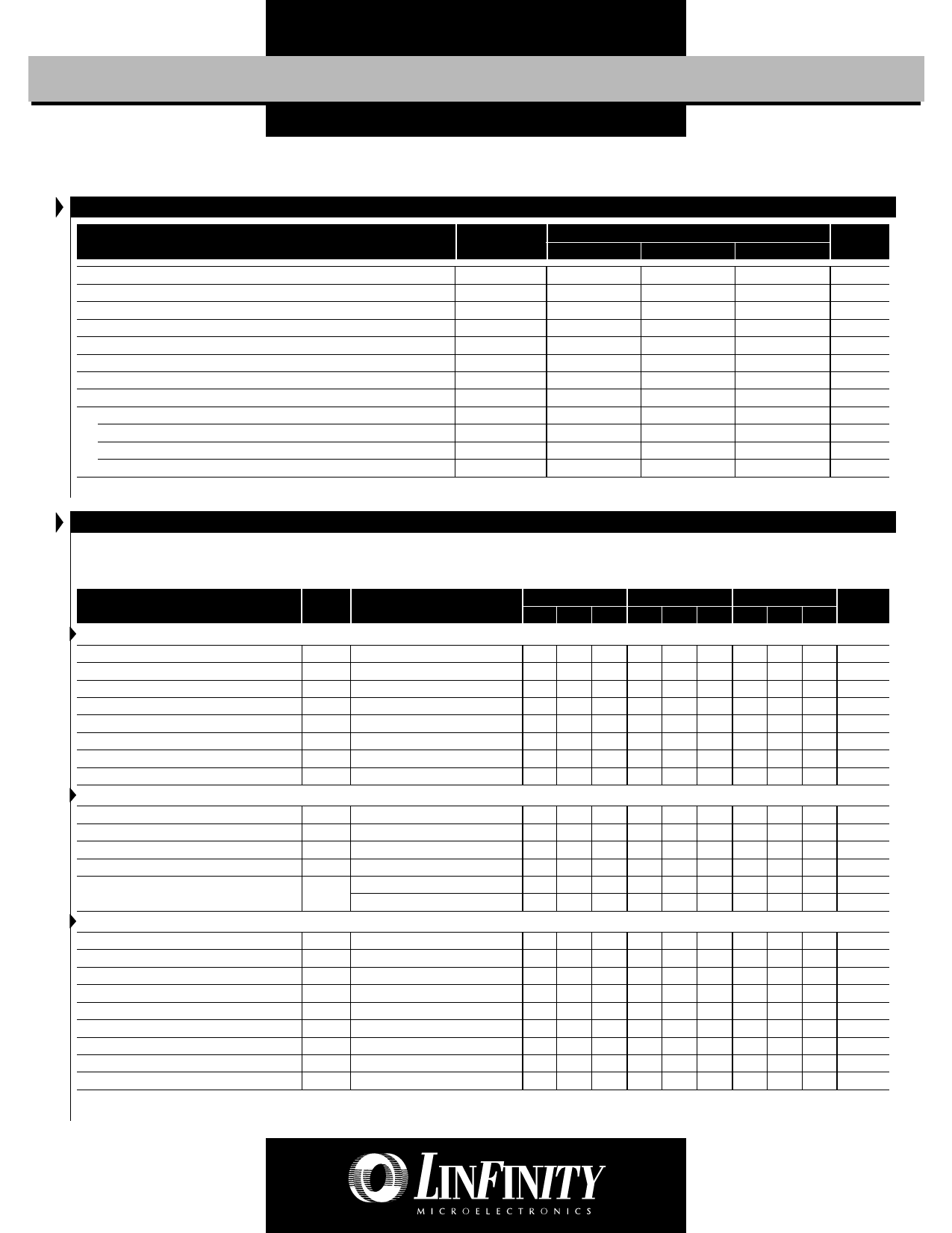
R E C O M M E N D E D O P E R A T I N G C O N D I T I O N S (Note 3)
Parameter
Symbol
Recommended Operating Conditions
Min.
Typ.
Max.
Supply Voltage Range
Output Current (Peak)
Output Current (Continuous)
Analog Inputs (Pin 2, Pin 3)
Error Amp Output Sink Current
Oscillator Frequency Range
Oscillator Timing Resistor
Oscillator Timing Capacitor
Operating Ambient Temperature Range:
SG1844/45
SG2844/45
SG3844/45
Note 3. Range over which the device is functional.
30
±1
200
0
2.6
5
0.1
500
RT
0.52
150
CT
0.1
1.0
-55
125
-25
85
0
70
Units
V
A
mA
V
mA
kHz
kΩ
µF
°C
°C
°C
ELECTRICAL CHARACTERISTICS
(Unless otherwise specified, these specifications apply over the operating ambient temperatures for SG1844/SG1845 with -55°C ≤ T ≤ 125°C, SG2844/
A
SG2845 with -25°C ≤ TA ≤ 85°C, SG3844/SG3845 with 0°C ≤ TA ≤ 70°C, VCC = 15V (Note 7), RT = 10kΩ, and CT = 3.3nF. Low duty cycle pulse testing
techniques are used which maintains junction and case temperatures equal to the ambient temperature.)
Parameter
Reference Section
Output Voltage
Line Regulation
Load Regulation
Temperature Stability (Note 4)
Total Output Variation (Note 4)
Output Noise Voltage (Note 4)
Long Term Stability (Note 4)
Output Short Circuit
Oscillator Section
Initial Accuracy (Note 8)
Voltage Stability
Temperature Stability (Note 4)
Amplitude
Discharge Current
Error Amp Section
Input Voltage
Input Bias Current
Open Loop Gain
Unity Gain Bandwidth (Note 4)
Power Supply Rejection Ratio
Output Sink Current
Output Source Current
VOUT High
VOUT Low
Symbol Test Conditions
SG1844/45
SG2844/45
SG3844/45 Units
Min. Typ. Max. Min. Typ. Max. Min. Typ. Max.
TJ = 25°C, IO = 1mA
12 ≤ VIN ≤ 25V
1 ≤ IO ≤ 20mA
4.95 5.00 5.05 4.95 5.00 5.05 4.90 5.00 5.10
6 20
6 20
6 20
6 25
6 25
6 25
0.2 0.4
0.2 0.4
0.2 0.4
V
mV
mV
mV/°C
Line, Load, Temp.
4.90
5.10 4.90
5.10 4.82
5.18 V
VN 10Hz ≤ f ≤ 10kHz, TJ = 25°C
50
50
50
µV
TA = 125°C, 1000hrs
5 25
5 25
5 25 mV
-30 -100 -180 -30 -100 -180 -30 -100 -180 mA
TJ = 25°C
12V ≤ VCC ≤ 25V
TMIN ≤ TA ≤ TMAX
VRT/CT (Peak to Peak)
TJ = 25°C
TMIN ≤ TA ≤ TMAX
47 52 57 47 52 57 47 52 57 kHz
.02 1
0.2 1
0.2 1
%
5
5
5
%
1.7
1.7
1.7
V
7.8 8.3 9.1 7.5 8.4 9.3 7.5 8.4 9.3 mA
6.8
9.3 7.2
9.5 7.2
9.5 mA
VCOMP = 2.5V
2.45 2.50 2.55 2.45 2.50
-0.3 -1
-0.3
AVOL
PSRR
2 ≤ VO ≤ 4V
TJ = 25°C
12 ≤ VCC ≤ 25V
VVFB = 2.7V, VCOMP = 1.1V
VVFB = 2.3V, VCOMP = 5V
VVFB = 2.3V, RL = 15K to gnd
VVFB = 2.7V, RL = 15K to VREF
65 90
65 90
0.7 1
0.7 1
60 70
60 70
26
26
-0.5 -0.8
-0.5 -0.8
56
56
0.7 1.1
0.7
(Electrical Characteristics continue next page.)
2.55
1
1.1
2.42
65
0.7
60
2
-0.5
5
2.50
-0.3
90
1
70
6
-0.8
6
0.7
2.58
-2
1.1
V
µA
dB
MHz
dB
mA
mA
V
V
Copyright © 2000
Rev. 1.4 4/00
3
Share Link: 