SG1846F/DESC 查看數據表(PDF) - Microsemi Corporation
零件编号
产品描述 (功能)
生产厂家
SG1846F/DESC Datasheet PDF : 10 Pages
| |||
SG1846
ABSOLUTE MAXIMUM RATINGS (Note 1 and 2)
Supply Voltage (+VIN) .......................................................... 40V
Collector Supply Voltage(VC) .............................................. 40V
Analog Inputs (Pins 3, 4, 5, 6, & 16) ...................... -0.3V to +VIN
Logic Input ........................................................... -0.3V to 5.5V
Soure/Sink Load current (continuous) .......................... 200mA
Source/Sink Load Current (peak, 200ns) ...................... 500mA
Reference Load Current .................................................. 30mA
Soft Start Sink Current ..................................................... 50mA
Note 1. Values beyond which damage may occur.
Note 2. Pin numbers refer to ceramic J package.
THERMAL DATA
J Package:
Thermal Resistance-Junction to Case, θJC .................. 30°C/W
Thermal Resistance-Junction to Ambient, θJA .............. 80°C/W
N Package:
Thermal Resistance-Junction to Case, θJC .................. 40°C/W
Thermal Resistance-Junction to Ambient, θJA ............. 65°C/W
DW Package:
Thermal Resistance-Junction to Case, θJC ................... 40°C/W
Thermal Resistance-Junction to Ambient, θJA ............. 95°C/W
F Package:
Thermal Resistance-Junction to Case, θJC .................. 70°C/W
Thermal Resistance-Junction to Ambient, θJA ........... 115°C/W
L Package:
Thermal Resistance-Junction to Case, θJC .................. 35°C/W
Thermal Resistance-Junction to Ambient, θJA ........... 120°C/W
Sync Output Current ........................................................... 5mA
Error Amplifier Output Current ............................................ 5mA
Oscillator Charging current (Pin 9) ..................................... 5mA
Operating Junction Temperature
Hermetic (J, L, F Packages) ........................................ 150°C
Plastic (N, DW Package) ............................................. 150°C
Storage Temperature Range ............................ -65°C to 150°C
Lead Temperature (Soldering, 10 Seconds) .................. 300°C
Note A.
Junction Temperature Calculation:
T
J
=
T
A
+
(P
D
x
θJA).
Note B. The above numbers for θJC are maximums for the limiting
thermal resistance of the package in a standard mount-
ing configuration. The θJA numbers are meant to be
guidelines for the thermal performance of the device/pc-
board system. All of the above assume no ambient
airflow.
RECOMMENDED OPERATING CONDITIONS (Note 3)
Supply Voltage Range ............................................... 8V to 40V
Collector Supply Voltage Range ............................. 4.5V to 40V
Source/Sink Output Current (continuous) ...................... 100mA
Source/Sink Output Current (peak 200ns) .................... 200mA
Reference Load Current ........................................... 0 to 10mA
Oscillator Frequency Range ........................... 1KHz to 500KHz
Note 3. Range over which the device is functional.
Oscillator Timing Resistor (RT) ........................... 2KΩ to 100KΩ
Oscillator Timing Capacitor (C ) .................... 1000 pF to 0.1µF
T
Operating Ambient Temperature Range
SG1846 ........................................................... -55°C to 125°C
SG2846 ............................................................. -25°C to 85°C
SG3846 ................................................................ 0°C to 70°C
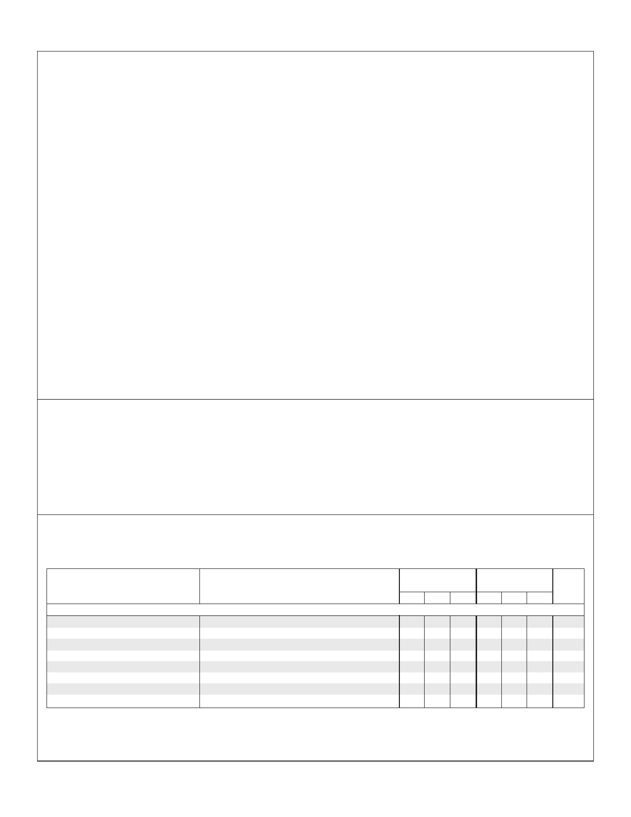
ELECTRICAL CHARACTERISTICS
(Unless otherwise specified, these specifications apply over the operating ambient temperatures for SG1846/SG1847 with -55°C ≤ TA ≤ 125°C, SG2846
with
-25°C
≤
T
A
≤
85°C,
SG3846
with
0°C
≤
T
A
≤
70°C,
+V
IN
=
15V.
Low duty cycle pulse testing techniques are used which maintains junction and
case temperatures equal to the ambient temperature.)
Parameter
Reference Section
Output Voltage
Line Regulation
Load Regulation
Temperature Stability (Note 4)
Total Output Variation (Note 4)
Output Noise Voltage (Note 4)
Long Term Stability (Note 4)
Short Circuit Output Current
Test Conditions
T = 25°C, I = 1mA
J
O
VIN = 8V to 40V
IL = 1mA to 10mA
Line, Load and Temperature
10Hz ≤ f ≤ 10KHz. TJ = 25°C
T = 125°C, 1000Hrs.
J
VREF = 0V
SG1846
SG2846
SG3846
Units
Min. Typ. Max. Min. Typ. Max.
5.05 5.10 5.15 5.00 5.10 5.20 V
5 20
5 20 mV
3 15
3 15 mV
0.4
0.4
mV/°C
5.00
5.20 4.95
5.25 V
100
100
µV
5
5
mV
-10 -45
-10 -45
mA
4/90 Rev 1.1 2/94
Copyright © 1994
LINFINITY Microelectronics Inc.
2
11861 Western Avenue ∞ Garden Grove, CA 92841
(714) 898-8121 ∞ FAX: (714) 893-2570
Share Link: 