SLY2016 ТЪЦуюІТЋИТЊџУАе№╝ѕPDF№╝Ѕ - Infineon Technologies
жЏХС╗Ху╝ќтЈи
С║ДтЊЂТЈЈУ┐░ (тіЪУЃй)
ућЪС║Дтјѓт«Х
SLY2016 Datasheet PDF : 5 Pages
| |||
AC Characteristics (guaranteed minimum timing
parameters at VCC=5.0 V ┬▒0.5 V)
Parameter
Symbol РђЊ40┬░C +25┬░C +85┬░C
Unit
Address Set
TAS
Up Time
10
10
10
ns
Write Time
TW
Data Set Up
TDS
Time
60
70
90
ns
20
30
50
ns
Address Hold TAH
Time
20
30
40
ns
Data Hold Time TDH
20
Access Time
TACC (1) 90
Clear Disable TCLRD 1.0
Time
30
40
ns
110 140 ns
1.0
1.0
┬хs
Clear Time
TCLR
1.0
1.0
1.0
ms
Note:
1) TACC=Set Up Time + Write Time + Hold Time
Loading Data
The desired data code (D0РђЊD6) and digit address (A0, A1) must
be held stable during the write cycle for storing new data.
Data entry may be asynchronous. Digit 0 is de№гЂned as right
hand digit with A1=A2=0.`
Clearing the entire internal four-digit memory can be accom-
plished by holding the clear (CLR) low for 1.0 msec minimum.
The clear function will clear the ASCII RAM. Loading an illegal
data code will display a blank.
Typical Loading State Table
WR A1 A0 D6 D5 D4 D3 D2 D1 D0 Digit
3210
H
previously loaded display
GRE Y
L L L H L L L H L H GRE E
L L H H L H L H L H GRUE
L H L H L L H H L L GL UE
L H H H L L L L H L BL UE
L L H H L L L H L H BL EE
L L L H L H L H H H BL EW
L X X see character code
see char. set
Display Blanking
Blank the display by loading a blank or space into each digit of
the display or by using the (BL) display blank input. Setting the
(BL) input low does not affect the contents of data memory.
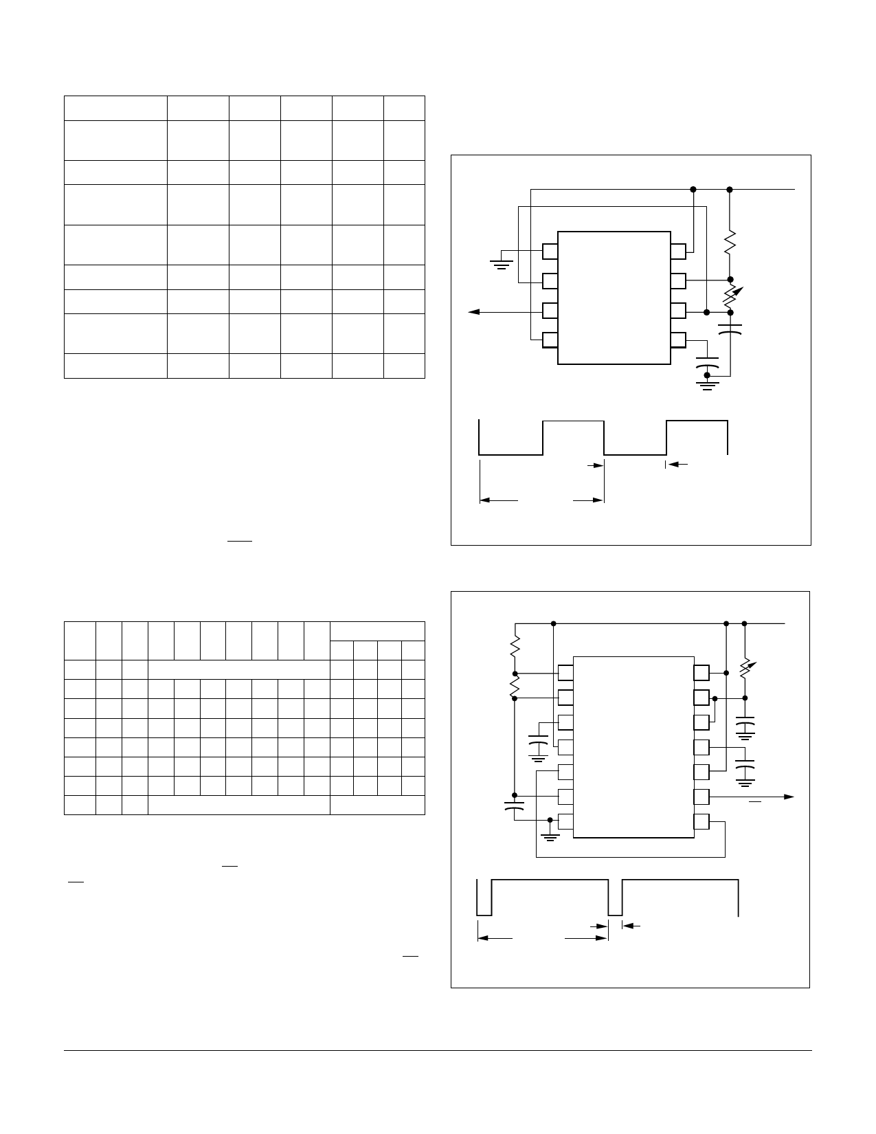
A №гѓashing circuit can easily be constructed using a 555 as table
multivibrator. Figure 3 illustrates a circuit in which varying R1
(100K~10K) will have a №гѓash rate of 1.0 Hz~10 Hz.
The display can be dimmed by pulse width modulating the (BL)
at a frequency suf№гЂciently fast to not interfere with the internal
clock. The dimming signal frequency should be 2.5 kHz or
higher. Dimming the display also reduces power consumption.
An example of a simple dimming circuit using a 556 is illus-
trated in Figure 4. Adjusting potentiometer R3 will dim the dis-
play by changing the blanking pulse duty cycle.
Figure 3. Flashing Circuit Using a 555 and Flashing
(Blanking) Timing
VCC=5.0 V
1
2
3
To BL
Pin on 4
Display
8
555
7
Timer
6
5
C4
0.01 ┬хF
R1
4.7 KРёд
R2
100 KРёд
C3
10 ┬хF
1
0
~~ 500 ms
~~2 Hz Blanking Frequency
Blanking Pulse Width
РЅѕ50% Duty Factor
Figure 4. Dimming Circuit Using a 556 and Dimming
(Blanking) Timing
R2
47 KРёд
1
R1
200Рёд
2
C2
0.01 ┬хF 3
4
5
C1
6
4700 pF
7
Dimming (Blanking)
Control
14
13
556
12
Dual Timer
11
10
9
8
VCC=5.0 V
R3
500 KРёд
C3
1000 pF
C4
0.01 ┬хF
To BL Pin
on Display
1
0
~~ 200 ┬хs
~~ 5 KHz Blanking Frequency
Blanking Pulse Width
4 ┬хs min., 196 ┬хs max.
№БЕ 2000 In№гЂneon Technologies Corp. Рђб Optoelectronics Division Рђб San Jose, CA
www.in№гЂneon.com/opto Рђб 1-888-In№гЂneon (1-888-463-4636)
OSRAM Opto Semiconductors GmbH & Co. OHG Рђб Regensburg, Germany
www.osram-os.com Рђб +49-941-202-7178
3
SLR/SLO/SLG/SLY2016
March 23, 2000-01
Share Link: 