744770933 查看數據表(PDF) - Diodes Incorporated.
零件编号
产品描述 (功能)
生产厂家
744770933 Datasheet PDF : 33 Pages
| |||
A Product Line of
Diodes Incorporated
ZXLD1370
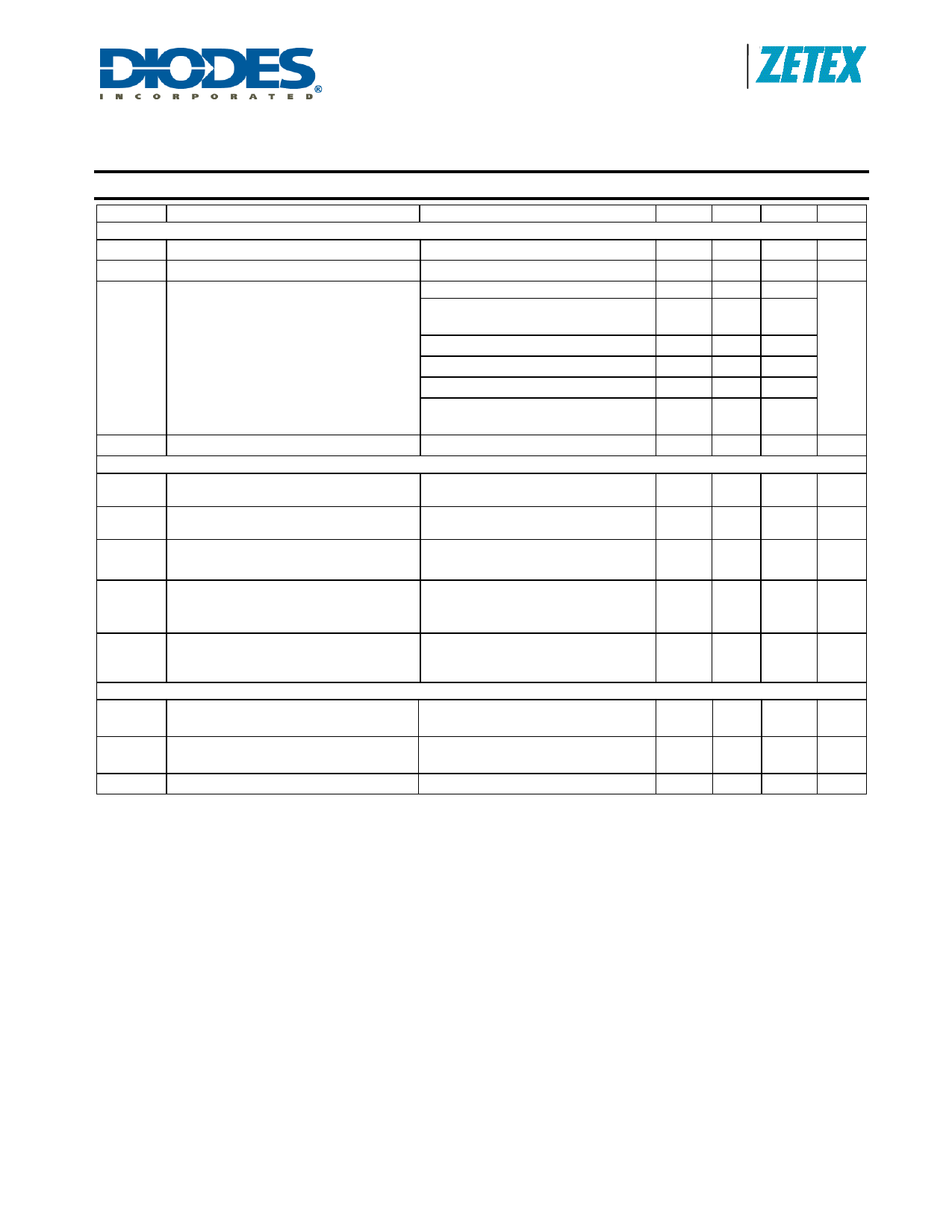
Electrical Characteristics (Test conditions: VIN = VAUX = 12V, TA = 25°C, unless otherwise specified.)
Symbol
Output Parameters
Parameter
Conditions
Min Typ Max Units
VFLAGL FLAG pin low level output voltage
IFLAGOFF FLAG pin open-drain leakage current
Output sinking 1mA
VFLAG=40V
Normal operation
0.5
V
1
µA
4.2 4.5 4.8
Out of regulation (VSHP out of range) 3.3
3.6
3.9
(Note 6)
VSTATUS
STATUS Flag no-load output voltage
(Note 5)
VIN under-voltage (VIN < 5.6V)
Switch stalled (tON or tOFF> 100µs)
3.3
3.3
3.6
3.6
3.9
3.9
V
Over-temperature (TJ > 125°C)
1.5 1.8 2.1
Excess sense resistor current
(VSENSE > 0.32V)
0.6 0.9 1.2
RSTATUS Output impedance of STATUS output Normal operation
10
kΩ
Driver output (PIN GATE)
VGATEH High level output voltage
No load Sourcing 1mA
(Note 7)
10
11
V
VGATEL Low level output voltage
Sinking 1mA, (Note 8)
0.5
V
VGATECL High level GATE CLAMP voltage
VIN = VAU X= VISM = 18V
IGATE = 1mA
12.8 15
V
Charging or discharging gate of
IGATE
Dynamic peak current available during
rise or fall of output voltage
external switch with QG = 10nC and
±300
mA
400kHz
Time to assert ‘STALL’ flag and
tSTALL warning on STATUS output
(Note 9)
GATE low or high
100 170 µs
LED Thermal control circuit (TADJ) parameters
VTADJH Upper threshold voltage
Onset of output current reduction
(VTADJ falling)
560 625 690 mV
VTADJL Lower threshold voltage
Output current reduced to <10% of 380 440 500 mV
set value (VTADJ falling)
ITADJ
TADJ pin Input current
VTADJ = 1.25V
1
µA
Notes:
5. In the event of more than one fault/warning condition occurring, the higher priority condition will take precedence. E.g. ‘Excessive coil current’ and
‘Out of regulation’ occurring together will produce an output of 0.9V on the STATUS pin. The voltage levels on the STATUS output assume the
Internal regulator to be in regulation and VADJ<=VREF. A reduction of the voltage on the STATUS pin will occur when the voltage on VIN is near the
minimum value of 6V.
6. Flag is asserted if VSHP<2.5V or VSHP>3.5V
7. GATE is switched to the supply voltage VAUX for low values of VAUX (i.e. between 6V and approximately 12V). For VAUX>12V, GATE is clamped
internally to prevent it exceeding 15V.
8. GATE is switched to PGND by an NMOS transistor
9. If tON exceeds tSTALL, the device will force GATE low to turn off the external switch and then initiate a restart cycle. During this phase, ADJ is
grounded internally and the SHP pin is switched to its nominal operating voltage, before operation is allowed to resume. Restart cycles will be
repeated automatically until the operating conditions are such that normal operation can be sustained. If tOFF exceeds tSTALL, the switch will remain
off until normal operation is possible.
ZXLD1370
Document number: DS32165 Rev. 2 - 2
5 of 33
www.diodes.com
May 2010
© Diodes Incorporated
Share Link: 