SN54-74LS169 查看數據表(PDF) - ON Semiconductor
零件编号
产品描述 (功能)
生产厂家
SN54-74LS169 Datasheet PDF : 6 Pages
| |||
SN54/74LS168 • SN54/74LS169
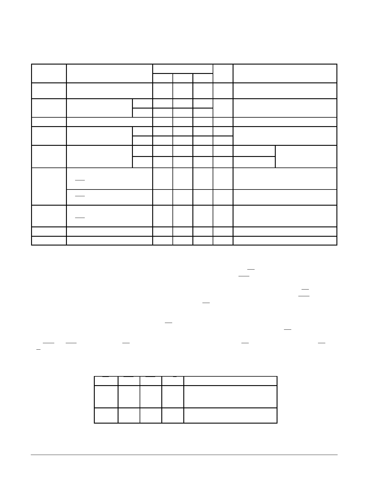
DC CHARACTERISTICS OVER OPERATING TEMPERATURE RANGE (unless otherwise specified)
Limits
Symbol
Parameter
Min Typ Max Unit
Test Conditions
VIH
Input HIGH Voltage
2.0
V
Guaranteed Input HIGH Voltage for
All Inputs
54
VIL
Input LOW Voltage
74
0.7
Guaranteed Input LOW Voltage for
0.8
V
All Inputs
VIK
VOH
Input Clamp Diode Voltage
54
Output HIGH Voltage
74
– 0.65 – 1.5
2.5
3.5
2.7
3.5
V
VCC = MIN, IIN = – 18 mA
V
VCC = MIN, IOH = MAX, VIN = VIH
V
or VIL per Truth Table
VOL
Output LOW Voltage
54, 74
74
0.25 0.4
0.35 0.5
V
IOL = 4.0 mA
V
IOL = 8.0 mA
VCC = VCC MIN,
VIN = VIL or VIH
per Truth Table
Input HIGH Current
Other Inputs
IIH
CET Input
Other Input
CET Input
20
µA VCC = MAX, VIN = 2.7 V
40
0.1
0.2
mA VCC = MAX, VIN = 7.0 V
Input LOW Current
IIL
Other Input
CET Input
– 0.4
– 0.8
mA VCC = MAX, VIN = 0.4 V
IOS
Short Circuit Current (Note 1)
– 20
– 100 mA VCC = MAX
ICC
Power Supply Current
34
mA VCC = MAX
Note 1: Not more than one output should be shorted at one time, nor for more than 1 second.
FUNCTIONAL DESCRIPTION
The SN54/74LS168 and SN54/74LS169 use edge-
triggered D-type flip-flops that have no constraints on
changing the control or data input signals in either state of the
Clock. The only requirement is that the various inputs attain
the desired state at least a set-up time before the rising edge of
the clock and remain valid for the recommended hold time
thereafter.
The parallel load operation takes precedence over the other
operations, as indicated in the Mode Select Table. When PE is
LOW, the data on the P0 – P3 inputs enters the flip-flops on the
next rising edge of the Clock. In order for counting to occur,
both CEP and CET must be LOW and PE must be HIGH. The
U/D input then determines the direction of counting.
The Terminal Count (TC) output is normally HIGH and goes
LOW, provided that CET is LOW, when a counter reaches zero
in the COUNT DOWN mode or reaches 15 (9 for the
SN54/74LS168) in the COUNT UP mode. The TC output state
is not a function of the Count Enable Parallel (CEP) input level.
The TC output of the SN54/74LS168 decade counter can also
be LOW in the illegal states 11, 13 and 15, which can occur
when power is turned on or via parallel loading. If illegal state
occurs, the SN54/74LS168 will return to the legitimate
sequence within two counts. Since the TC signal is derived by
decoding the flip-flop states, there exists the possibility of
decoding spikes on TC. For this reason the use of TC as a
clock signal is not recommended.
PE
CEP
L
X
H
L
H
L
H
H
H
X
H = HIGH Voltage Level
L = LOW Voltage Level
X = Immaterial
MODE SELECT TABLE
CET
U/D
Action on Rising Clock Edge
X
X
Load (Pn → Qn)
L
H
Count Up (increment)
L
L
Count Down (decrement)
X
X
No Change (Hold)
H
X
No Change (Hold)
FAST AND LS TTL DATA
5-4
Share Link: 