SN74LS247DW 查看數據表(PDF) - Motorola => Freescale
零件编号
产品描述 (功能)
生产厂家
SN74LS247DW Datasheet PDF : 8 Pages
| |||
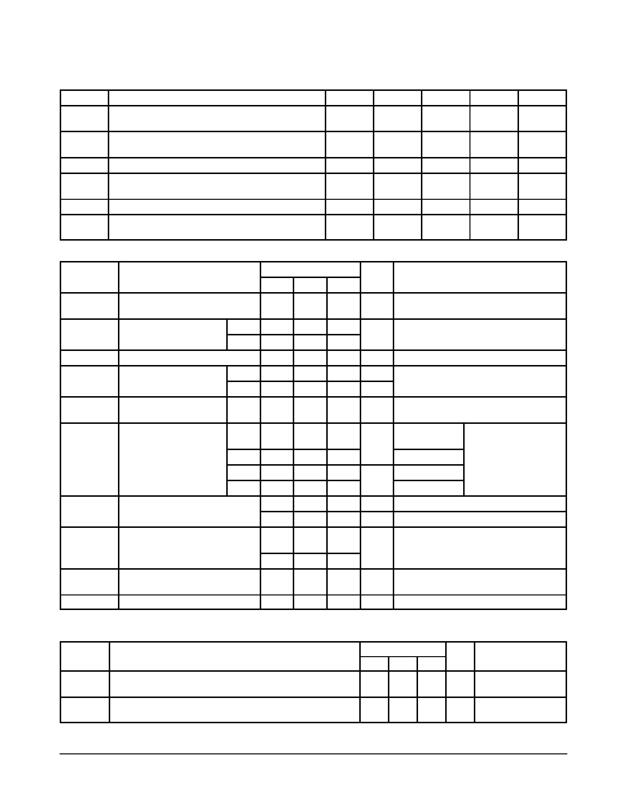
SN54 / 74LS249
GUARANTEED OPERATING RANGES
Symbol
Parameter
VCC
Supply Voltage
TA
Operating Ambient Temperature Range
IOH
IOL
VOH
IOL
Output Current — High BI / RBO
Output Current — Low BI / RBO
Output Current — Low BI / RBO
Output Voltage — High a – g
Output Current — Low a – g
Output Current — Low a – g
Min
Typ
Max
Unit
54
4.5
5.0
5.5
V
74
4.75
5.0
5.25
54
– 55
25
125
°C
74
0
25
70
54, 74
– 50
µA
54
1.6
mA
74
3.2
54, 74
5.5
V
54
4.0
mA
74
8.0
DC CHARACTERISTICS OVER OPERATING TEMPERATURE RANGE (unless otherwise specified)
Limits
Symbol
Parameter
Min Typ Max Unit
Test Conditions
VIH
Input HIGH Voltage
2.0
Guaranteed Input HIGH Voltage for
V All Inputs
54
VIL
Input LOW Voltage
74
0.7
Guaranteed Input LOW Voltage for
0.8
V All Inputs
VIK
VOH
Input Clamp Diode Voltage
Output HIGH Voltage
54
BI / RBO
74
– 0.65 – 1.5
2.4
4.2
2.4
4.2
V VCC = MIN, IIN = – 18 mA
V VCC = MIN, IOH = MAX, VIN = VIH
V or VIL per Truth Table
IOH
VOL
IIH
IIL
Output HIGH Current
a–g
54, 74
Output LOW Voltage
BI / RBO
54, 74
74
a–g
54, 74
74
Input HIGH Current
Any Input, except BI/ RBO
Input LOW Current
Any Input, except BI/ RBO
BI / RBO
250
µA
VCC = MIN, VIH = 2.0 V,
VOH = 5.5 V, VIL = MAX
0.25 0.4
0.35 0.5
0.25 0.4
0.35 0.5
20
0.1
V IOL = 1.6 mA
IOL = 3.2 mA
IOL = 4.0 mA
V
IOL = 8.0 mA
VCC = MIN, VIH = 2.0 V,
VIL = per Truth Table
µA VCC = MAX, VIN = 2.7 V
mA VCC = MAX, VIN = 7.0 V
– 0.4
– 1.2
mA VCC = MAX, VIN = 0.4 V
IOS
Short Circuit Current
BI / RBO (Note 1)
– 0.3
– 2.0 mA VCC = MAX
ICC
Power Supply Current
8.0
15
Note 1: Not more than one output should be shorted at a time, nor for more than 1 second.
mA VCC = MAX
AC CHARACTERISTICS (VCC = 5.0 V, TA = 25°C)
Symbol
tPHL
tPLH
tPHL
tPLH
Parameter
Propagation Delay Time, High-to-Low-Level Output from A Input
Propagation Delay Time, Low-to-High-Level Output from A Input
Propagation Delay Time, High-to-Low-Level Output from RBI Input
Propagation Delay Time, Low-to-High-Level Output from RBI Input
Limits
Min Typ Max
100
100
100
100
Unit
Test Conditions
ns CL = 15 pF, RL = 2.0 Ω
ns CL = 15 pF, RL = 6.0 Ω
FAST AND LS TTL DATA
5-407
Share Link: 