SP312A 查看數據表(PDF) - Signal Processing Technologies
零件编号
产品描述 (功能)
生产厂家
SP312A Datasheet PDF : 8 Pages
| |||
Receivers
The receivers convert RS-232 input signals to
inverted TTL signals. Since the input is usually
from a transmission line, where long cable lengths
and system interference can degrade the signal, the
inputs have a typical hysteresis margin of 500mV.
This ensures that the receiver is virtually immune
to noisy transmission lines.
The input thresholds are 0.8V minimum and
2.4V maximum, again well within the ±3V
RS-232 requirements. The receiver inputs are also
protected against voltages up to ±30V. Should an
input be left unconnected, a 5kOhm pulldown
resistor to ground will commit the output of the
receiver to a high state.
In actual system applications, it is quite possible
for signals to be applied to the receiver inputs
before power is applied to the receiver circuitry.
This occurs, for example, when a PC user attempts
to print, only to realize the printer wasn’t turned on.
In this case an RS-232 signal from the PC will
appear on the receiver input at the printer. When
the printer power is turned on, the receiver will
operate normally. All of these enhanced devices
are fully protected.
Charge Pump
The charge pump section of the these devices
allows the circuit to operate from a single +5V
±10% power supply by generating the required
operating voltages internal to the devices. The
charge pump consists of two sections — 1) a
voltage doubler and 2) a voltage inverter.
As shown in Figure 1, an internal oscillator trig-
gers the charge accumulation and voltage inver-
sion. The voltage doubler momentarily stores a
charge on capacitor C1 equal to Vcc, referenced to
ground. During the next transition of the oscillator
this charge is boot-strapped to transfer charge to
cVacpcatcoitVor+.C3. The voltage across C3 is now from
In the inverter section (Figure 2), the voltage
attorcarnVoss+fseaCrcc3rhoisastrsrgaCen2ts.ofeBCror4eodtto-tsogtreCanp2rpfaotienrcgVino-g.f
a range of 0V
C2 will then
One of the significant enhancements over
previous products of this type is that the values of
the capacitors are no longer critical and have been
decreased in size considerably to 0.1µF. Because
the charge pump runs at a much higher frequency,
the 0.1µF capacitors are sufficient to transfer and
sustain charges to the two transmitters.
APPLICATION HINTS
Protection From Shorts to ±15V
The driver outputs are protected against shorts
to ground, other driver outputs, and V+ or V-.
If the possibility exists that the outputs could be
inadvertently connected to voltages higher than
±15V, then it is recommended that external
protection be provided. For protection against
voltages exceeding ±15V, two back-to-back zener
diodes connected from each output to ground will
clamp the outputs to an acceptable voltage level.
+5V INPUT
V+ (+8.5V to +13.2V)
1
0.1µ F +
C 1+
6.3V
2 C 1-
13
V CC
+12V to -12V
Voltage Inverter
14
V+
0.1µ F
16V
V- 3 +
T1 IN
8
T2 IN
7
400k Ω
T1
400k Ω
T2
11
T 1OUT
4
T 2OUT
R1OUT
9
R1
10
R 1IN
5k Ω
R2OUT
6
R2
5
R 2IN
SP231A
5k Ω
GND 12
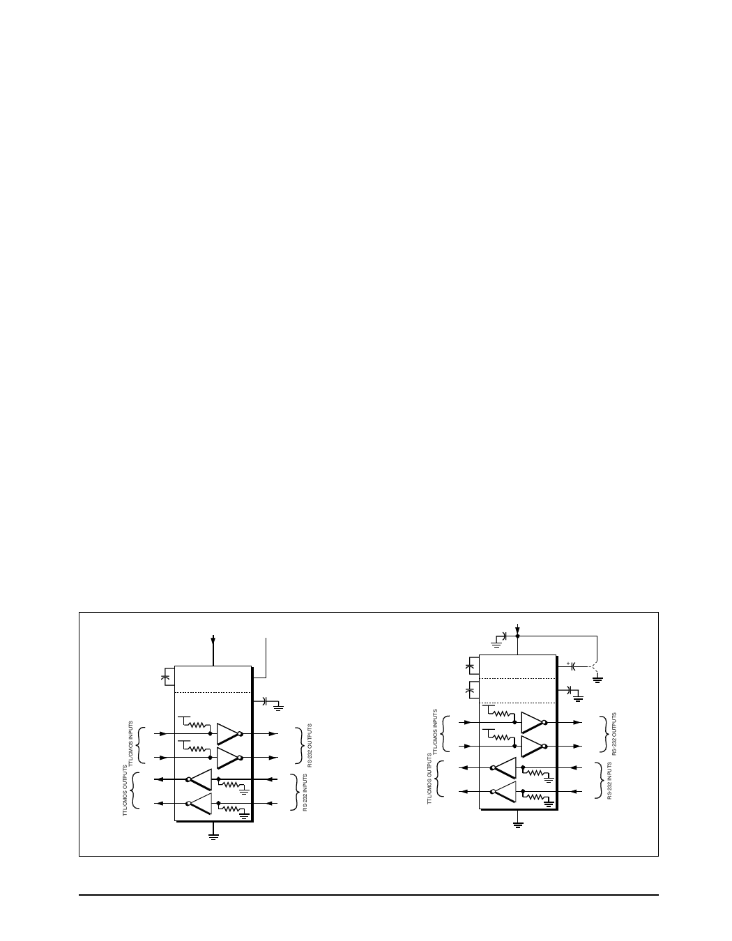
Figure 3. Typical Circuits using the SP231A and 232A.
+5V INPUT
10 µF 6.3V
+
1
0.1µ F +
C 1+
6.3V
3 C 1-
4
0.1µ F +
C 2+
16V
5 C 2-
16
V CC
+5V to +10V
Voltage Doubler
+10V to -10V
Voltage Inverter
T1 IN
11
T2 IN
10
400k Ω
T1
400k Ω
T2
0.1µ F 6.3V
2
V+
*
V- 6 + 0.1µ F
16V
14
T 1OUT
7
T 2OUT
R1OUT
12
R1
13
R 1IN
5k Ω
R2OUT
9
R2
8
R 2IN
SP232A
5k Ω
GND 15
*The negative terminal of the V+ storage capacitor can be tied
to either VCC or GND. Connecting the capacitor to VCC (+5V)
is recommended.
SP231ADS/01
SP231A Enhanced RS-232 Line Drivers/Receivers
5
© Copyright 2000 Sipex Corporation
Share Link: 