ICL7673CPA(1999) 查看數據表(PDF) - Intersil
零件编号
产品描述 (功能)
生产厂家
ICL7673CPA Datasheet PDF : 7 Pages
| |||
ICL7673
Typical Performance Curves (Continued)
1
5
VO = 5V
VO = 9V
0.8
4
VO = 3V
VO = 12V
0.6
3
0.4
0.2
-284550oooCCC
02
4 6 8 10 12 14 16
SUPPLY VOLTAGE (V)
FIGURE 3. SUPPLY CURRENT AS A FUNCTION OF SUPPLY
VOLTAGE
1mA
100mA
10nA
1nA
ILOAD = 10mA
VS = 0V
85oC
1000pA
10pA
25oC
1pA
0
2
4 56
8
10
12
INPUT VP (V)
FIGURE 5. IS LEAKAGE CURRENT VP TO VS AS A
FUNCTION OF INPUT VOLTAGE
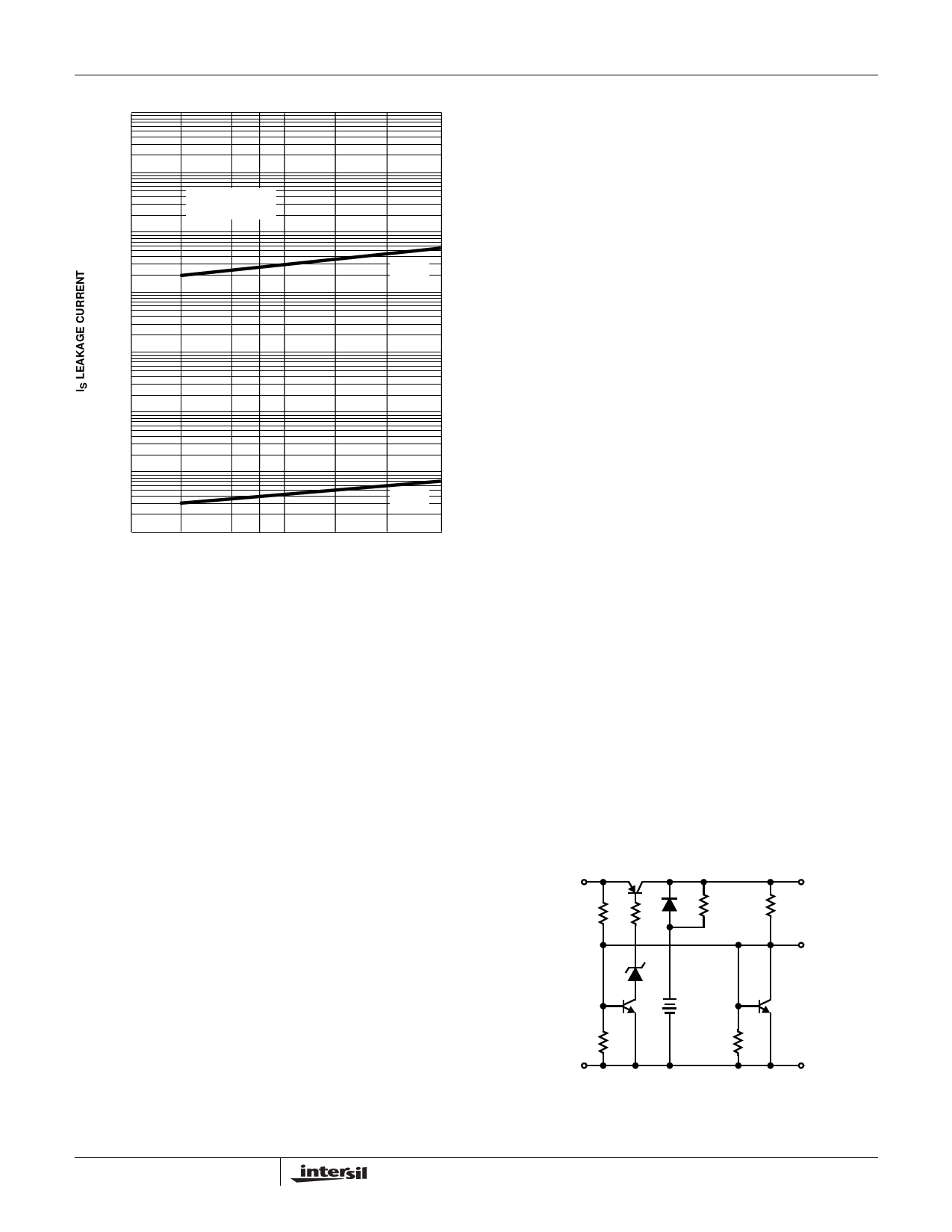
Detailed Description
As shown in the Functional Diagram, the ICL7673 includes a
comparator which senses the input voltages VP and VS. The
output of the comparator drives the first inverter and the
open-drain N-Channel transistor PBAR . The first inverter
drives a large P-Channel switch, P1, a second inverter, and
another open-drain N-Channel transistor, SBAR . The second
2
VO = 15V
1
0
40
80
120
140
180
OUTPUT CURRENT (mA)
FIGURE 4. PBAR OR SBAR SATURATION VOLTAGE AS A
FUNCTION OF OUTPUT CURRENT
inverter drives another large P-Channel switch P2. The
ICL7673, connected to a main and a backup power supply,
will connect the supply of greater potential to its output. The
circuit provides break-before-make switch action as it
switches from main to backup power in the event of a main
power supply failure. For proper operation, inputs VP and VS
must not be allowed to float, and, the difference in the two
supplies must be greater than 50mV. The leakage current
through the reverse biased parasitic diode of switch P2 is
very low.
Output Voltage
The output operating voltage range is 2.5V to 15V. The
insertion loss between either input and the output is a
function of load current, input voltage, and temperature. This
is due to the P-Channels being operated in their triode
region, and, the ON-resistance of the switches is a function
of output voltage VO. The ON-resistance of the P-Channels
have positive temperature coefficients, and therefore as
temperature increases the insertion loss also increases. At
low load currents the output voltage is nearly equal to the
greater of the two inputs. The maximum voltage drop across
switch P1 or P2 is 0.5V, since above this voltage the body-
drain parasitic diode will become forward biased. Complete
switching of the inputs and open-drain outputs typically
occurs in 50µs.
Input Voltage
The input operating voltage range for VP or VS is 2.5V to
15V. The input supply voltage (VP or VS) slew rate should be
limited to 2V per microsecond to avoid potential harm to the
circuit. In line-operated systems, the rate-of-rise (or fall) of
the supply is a function of power supply design. For battery
applications it may be necessary to use a capacitor between
the input and ground pins to limit the rate-of-rise of the
3-84
Share Link: 