SP6681EU 查看數據表(PDF) - Signal Processing Technologies
零件编号
产品描述 (功能)
生产厂家
SP6681EU Datasheet PDF : 10 Pages
| |||
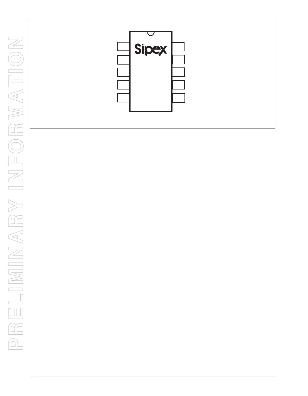
PINOUT
VOUT 1
CF1P 2
VIN 3
C/4 4
Cx8 5
SP6681
10 CF2P
9 CF1N
8 GND
7 CF2N
6 CLK
PIN ASSIGNMENTS
Pin 1— VOUT — 5.0V regulated charge pump.
Pin 2 — CF1P — Positive terminal to the charge
pump flying capacitor, CF1.
Pin 3 — VIN — Input pin for the +2.7V to +5.5V
supply voltage.
Pin 4 — C/4 — This is a control line for the
internal charge pump frequency. When this
control line is forced to a logic high, the
internal charge pump frequency is set to 1/4 of
the CLK frequency, provided that Cx8 is
low.
Pin 5 — Cx8 — This is a control line for the
internal charge pump frequency. When this
control line is forced to a logic high, the
internal charge pump frequency is set to x8 of
the CLK frequency.
Pin 6 — CLK — 32.768kHz Clock. Connect
this input pin to an external 32.768kHz clock
to drive the frequency of the charge pump.
Logic low inputs on the C/4 and Cx8 pins sets
the internal charge pump frequency accord-
ing to Table 1. Shutdown mode for the
device is set when there is no clock signal
present on this input pin, or when it is pulled
to ground.
Pin 7 — CF2N — Negative terminal to the
charge pump flying capacitor, CF2.
Pin 8 — GND — Ground reference.
Pin 9 — CF2P — Positive terminal to the charge
pump flying capacitor, CF2.
Pin 10 — CF1N — Negative terminal to the
charge pump flying capacitor, CF2.
Rev:A Date: 11/20/03
SP6681 High Efficiency Boost Charge Pump Regulator
4
© Copyright 2002 Sipex Corporation
Share Link: 