SP6686ER-L/TR 查看數據表(PDF) - Signal Processing Technologies
零件编号
产品描述 (功能)
生产厂家
SP6686ER-L/TR Datasheet PDF : 13 Pages
| |||
VIN , VOUT ...................................................................... -0.3V to 6V
Output Current Pulse (Flash) .......................... 500mA
Output Current Continuous (Torch) ................. 200mA
Storage Temperature ...................... -65°C to +150°C
Operating Temperature ..................... -40°C to +85°C
VEN ......................................................... ZeroV to 7V
3x3 10 DFN .........................................OJA = 57.1°C/W
ESD Rating. ................................................ 2kV HBM
ABSOLUTE MAXIMUM RATINGS
These are stress ratings only and functional operation of
the device at these ratings or any other above those
indicated in the operation sections of the specifications
below is not implied. Exposure to absolute maximum
rating conditions for extended periods of time may affect
reliability.
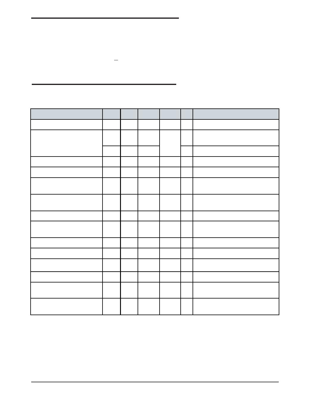
ELECTRICAL CHARACTERISTICS
TA = -40°C to +85°C, VIN = 3.6, CIN = 2.2µF, CFC = 0.47µF, COUT = 1.0µF. VSHDN = VIN, typical values at 25°C. The
♦ denotes the specifications which apply over the full operating range unless otherwise noted.
PARAMETER
Operating Input Voltage
Quiescent Current
Shutdown Current
Oscillator Frequency
Charge Pump Equivalent
Resistance (x2 mode)
Charge Pump Equivalent
Resistance (x1 mode)
FB Reference Voltage
FB Reference Voltage
MIN. TYP.
2.7
0.5
2
2.4
5
MAX.
5.5
3
1
UNITS
V♦
mA ♦
µA
MHz
Ω
CONDITIONS
VIN = 2.7 - 5.5V FLASH = 0Volts,
Iload = 100µA
FLASH = VIN, 2x mode
V
IN
=
5.5V,
VEN
=
0Volts
V
FB
=
0Volts,
VIN=
3.6V
0.6
0.8
Ω
VIN= 3.6V
138 150 162
45 50
55
mV
♦
FLASH = VIN
R=
SET
106KΩ
mV ♦ FLASH = GND
FB Pin Current
EN, FLASH Logic Low
EN, FLASH Logic High
EN, FLASH Pin Current
V Turn-on Time
OUT
Thermal Shutdown
Temperature
0.5
0.4
1.3
0.5
250 500
145
µA
VFB = 0.3V
V♦
V♦
µA ♦
µs
♦
V = 3.6V, FB within 90% of
IN
regulation
ºC
Date: 03/10/06
SP6686 400mA, Buck/Boost Charge Pump LED Driver
2
© Copyright 2006 Sipex Corporation
Share Link: 