SST27SF010 查看數據表(PDF) - Silicon Storage Technology
零件编号
产品描述 (功能)
生产厂家
SST27SF010
Silicon Storage Technology

SST27SF010 Datasheet PDF : 26 Pages
| |||
256 Kbit / 512 Kbit / 1 Mbit / 2 Mbit Multi-Purpose Flash
SST27SF256 / SST27SF512 / SST27SF010 / SST27SF020
Data Sheet
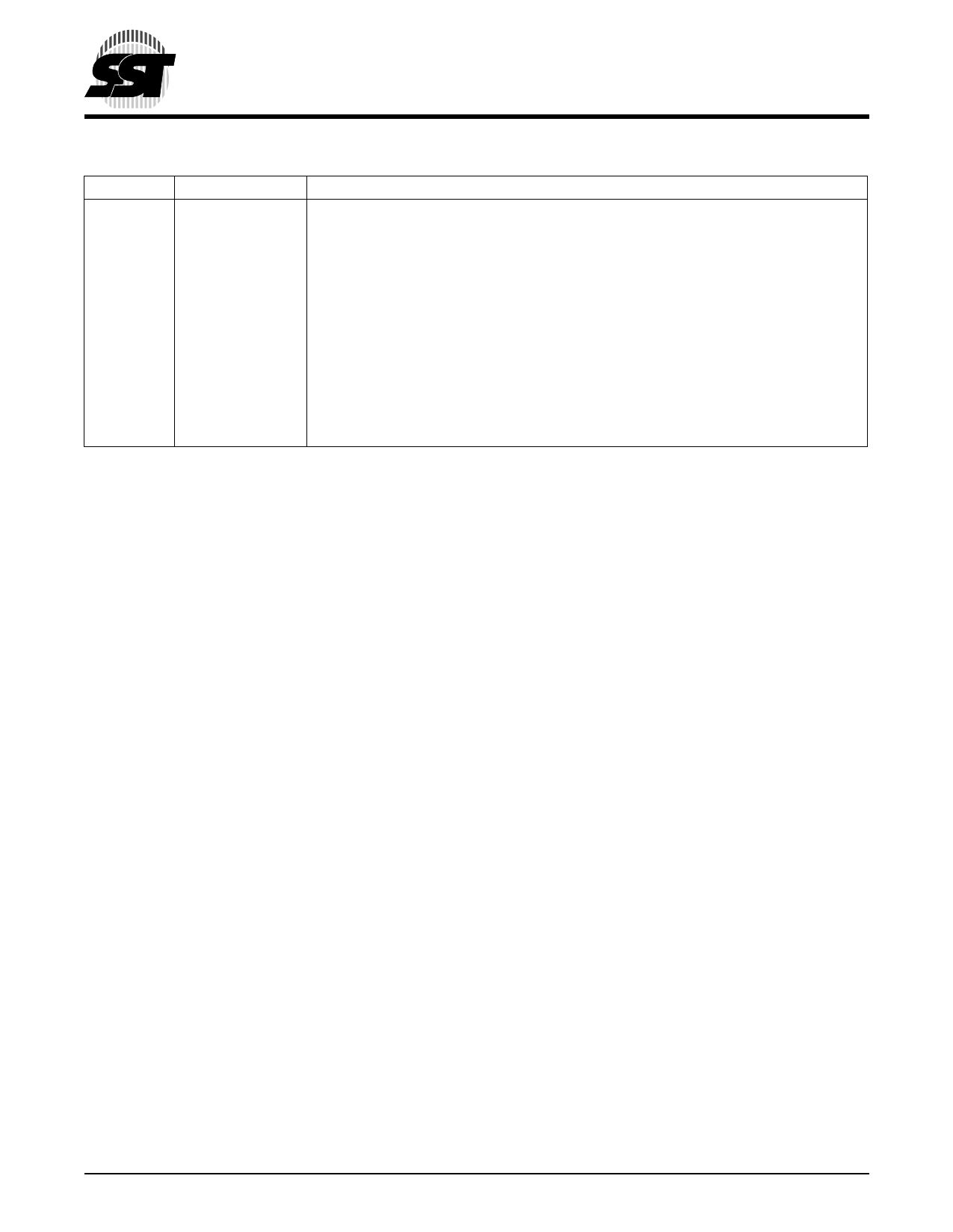
TABLE 2: PIN DESCRIPTION
Symbol
AMS1-A0
DQ7-DQ0
Pin Name
Address Inputs
Data Input/output
Functions
To provide memory addresses
To output data during Read cycles and receive input data during Program cycles
The outputs are in tri-state when OE# or CE# is high.
CE#
Chip Enable
To activate the device when CE# is low
OE#
Output Enable
For SST27SF256/010/020, to gate the data output buffers during Read operation
OE#/VPP
Output Enable/VPP For SST27SF512, to gate the data output buffers during Read operation and high voltage
pin during Chip-Erase and programming operation
VPP
Power Supply for For SST27SF256/010/020, high voltage pin during Chip-Erase and programming opera-
Program or Erase tion 12V (±5%)
VDD
Power Supply
To provide 5.0V supply (±10%)
VSS
Ground
NC
No Connection
Unconnected pins.
1. AMS = Most significant address
AMS = A14 for SST27SF256, A15 for SST27SF512, A16 for SST27SF010, and A17 for SST27SF020
T2.3 502
©2001 Silicon Storage Technology, Inc.
6
S71152-02-000 5/01 502
Share Link: