STK11C88-3SF35I 查看數據表(PDF) - Simtek Corporation
零件编号
产品描述 (功能)
生产厂家
STK11C88-3SF35I Datasheet PDF : 10 Pages
| |||
STK11C88-3
ABSOLUTE MAXIMUM RATINGSa
Voltage on Input Relative to Ground . . . . . . . . . . . . . .–0.5V to 4.5V
Voltage on Input Relative to VSS . . . . . . . . . . –0.6V to (VCC + 0.5V)
Voltage on DQ0-7 . . . . . . . . . . . . . . . . . . . . . . –0.5V to (VCC + 0.5V)
Temperature under Bias . . . . . . . . . . . . . . . . . . . . . –55°C to 125°C
Storage Temperature . . . . . . . . . . . . . . . . . . . . . . . –65°C to 150°C
Power Dissipation . . . . . . . . . . . . . . . . . . . . . . . . . . . . . . . . . . . . 1W
DC Output Current (1 output at a time, 1s duration) . . . . . . . . 15mA
Note a:
Stresses greater than those listed under “Absolute Maximum
Ratings” may cause permanent damage to the device. This is a
stress rating only, and functional operation of the device at condi-
tions above those indicated in the operational sections of this
specification is not implied. Exposure to absolute maximum rat-
ing conditions for extended periods may affect reliability.
DC CHARACTERISTICS
(VCC = 3.0V-3.6V)
SYMBOL
ICC1b
PARAMETER
Average VCC Current
ICC2c
ICC3b
ISB1d
ISB2d
IILK
IOLK
VIH
VIL
VOH
VOL
TA
Average VCC Current During STORE
Average VCC Current at tAVAV = 200ns
3.3V, 25°C, Typical
Average VCC Current
(Standby, Cycling TTL Input Levels)
VCC Standby Current
(Standby, Stable CMOS Input Levels)
Input Leakage Current
Off-State Output Leakage Current
Input Logic “1” Voltage
Input Logic “0” Voltage
Output Logic “1” Voltage
Output Logic “0” Voltage
Operating Temperature
COMMERCIAL
MIN
MAX
50
42
37
3
9
18
16
15
750
INDUSTRIAL
MIN MAX
52
44
39
3
UNITS
mA
mA
mA
mA
9
mA
19
mA
17
mA
16
mA
750
μA
±1
±1
μA
±1
±1
μA
2.2
VCC + .5 2.2 VCC + .5 V
VSS – .5
0.8 VSS – .5 0.8
V
2.4
2.4
V
0.4
0.4
V
0
70
– 40
85
°C
NOTES
tAVAV = 35ns
tAVAV = 45ns
tAVAV = 55ns
All Inputs Don’t Care, VCC = max
W ≥ (VCC – 0.2V)
All Others Cycling, CMOS Levels
tAVAV = 35ns, E ≥ VIH
tAVAV = 45ns, E ≥ VIH
tAVAV = 55ns, E ≥ VIH
E ≥ (VCC - 0.2V)
All Others VIN ≤ 0.2V or ≥ (VCC – 0.2V)
VCC = max
VIN = VSS to VCC
VCC = max
VIN = VSS to VCC, E or G ≥ VIH
All Inputs
All Inputs
IOUT = – 4mA
IOUT = 8mA
Note b: ICC1 and ICC3 are dependent on output loading and cycle rate. The specified values are obtained with outputs unloaded.
Note c: ICC2 is the average current required for the duration of the STORE cycle (tSTORE ) .
Note d: E ≥ VIH will not produce standby current levels until any nonvolatile cycle in progress has timed out.
AC TEST CONDITIONS
3.3V
Input Pulse Levels . . . . . . . . . . . . . . . . . . . . . . . . . . . . . .0V to 3.0V
Input Rise and Fall Times . . . . . . . . . . . . . . . . . . . . . . . . . . . . . . . ≤ 5ns
Input and Output Timing Reference Levels . . . . . . . . . . . . . . . 1.5V
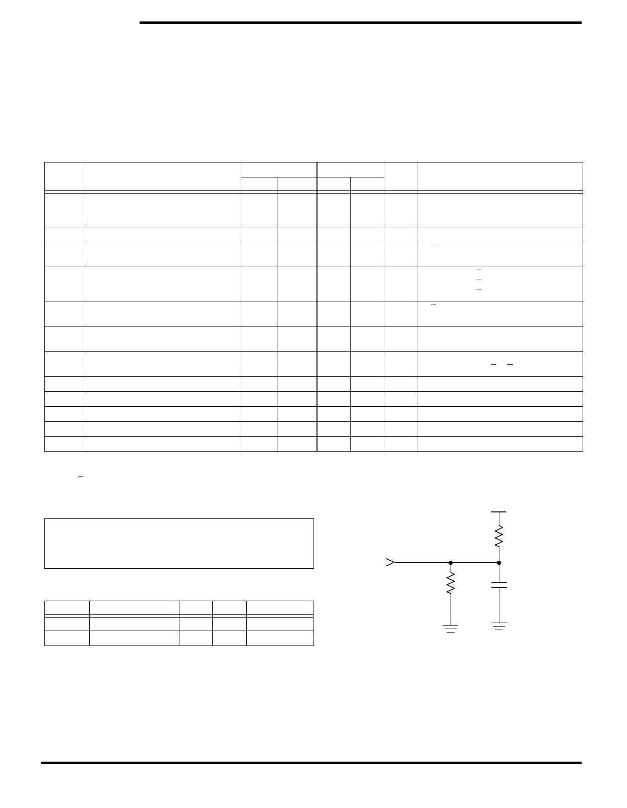
Output Load . . . . . . . . . . . . . . . . . . . . . . . . . . . . . . . . . See Figure 1
CAPACITANCEe (TA = 25°C, f = 1.0MHz)
SYMBOL
CIN
COUT
PARAMETER
Input Capacitance
Output Capacitance
MAX
5
7
UNITS
pF
pF
CONDITIONS
ΔV = 0 to 3V
ΔV = 0 to 3V
Note e: These parameters are guaranteed but not tested.
OUTPUT
351 Ohms
317 Ohms
30 pF
INCLUDING
SCOPE AND
FIXTURE
Figure 1: AC Output Loading
March 2006
2 Document Control # ML0013 rev 0.2
Share Link: 