STK14CA8 查看數據表(PDF) - Cypress Semiconductor
零件编号
产品描述 (功能)
生产厂家
STK14CA8 Datasheet PDF : 16 Pages
| |||
STK14CA8
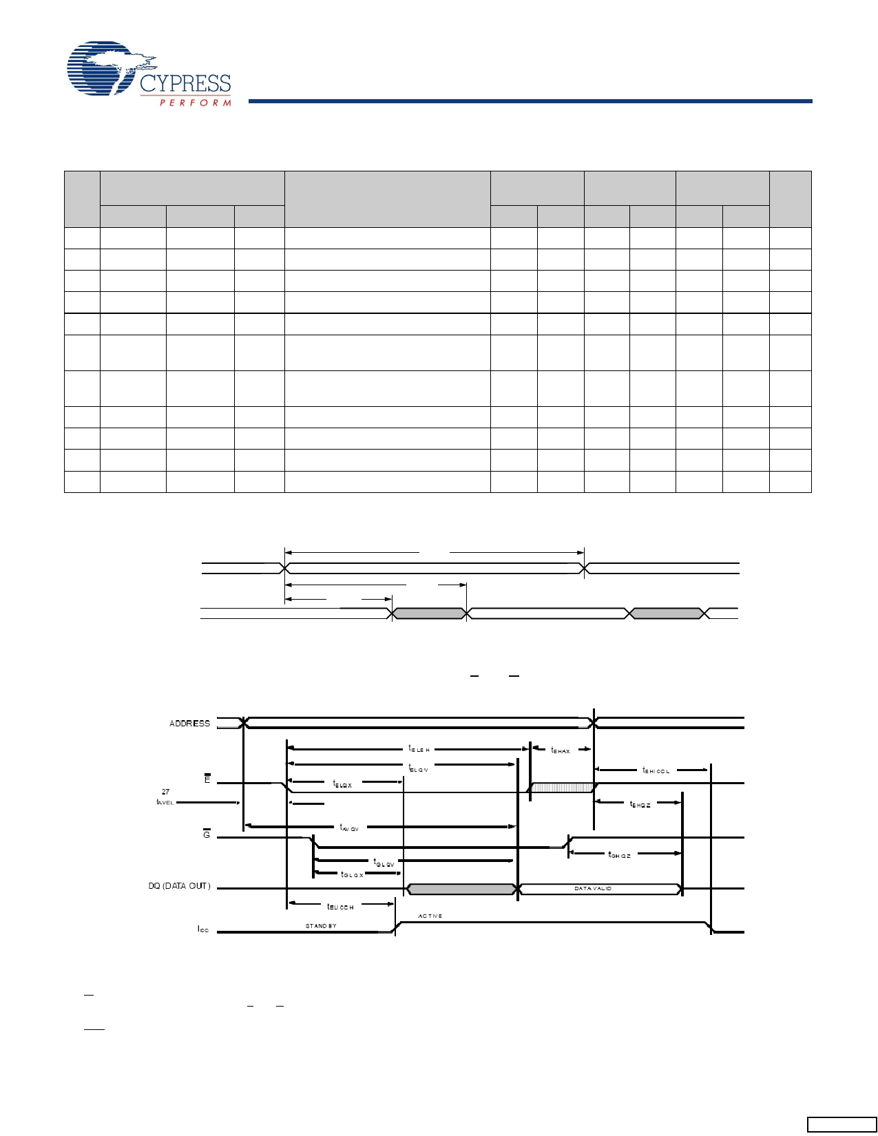
SRAM READ Cycles #1 and #2
NO.
#1
1
2 tAVAV[3]
3 tAVQV[4]
4
5 tAXQX[4]
6
7
8
9
10
11
Symbols
#2
tELQV
tELEH[3]
tAVQV[4]
tGLQV
tAXQX[4]
tELQX
tEHQZ[5]
Alt.
tACS
tRC
tAA
tOE
tOH
tLZ
tHZ
tGLQX
tGHQZ[5]
tELICCH[2]
tEHICCL[2]
tOLZ
tOHZ
tPA
tPS
Parameter
STK14CA8-25 STK14CA8-35 STK14CA8-45
Units
Min Max Min Max Min Max
Chip Enable Access Time
25
35
45 ns
Read Cycle Time
25
35
45
ns
Address Access Time
25
35
45 ns
Output Enable to Data Valid
12
15
20 ns
Output Hold after Address Change 3
3
3
ns
Address Change or Chip Enable to 3
3
3
ns
Output Active
Address Change or Chip Disable to
10
13
15 ns
Output Inactive
Output Enable to Output Active
0
0
0
ns
Output Disable to Output Inactive
10
13
15 ns
Chip Enable to Power Active
0
0
0
ns
Chip Disable to Power Standby
25
35
45 ns
ADDRESS
DQ (DATA OUT)
Figure 6. SRAM READ Cycle #1: Address Controlled[3, 4, 6]
2
tAVAV
5
tAXQX
3
tAVQV
DATA VALID
Figure 7. SRAM READ Cycle #2: E and G Controlled[3, 6]
2
1
6
3
4
8
10
29
11
7
9
Notes
3. W must be high during SRAM READ cycles.
4. Device is continuously selected with E and G both low
5. Measured ± 200mV from steady state output voltage.
6. HSB must remain high during READ and WRITE cycles
Document Number: 001-51592 Rev. **
Page 5 of 16
[+] Feedback
Share Link: 