STK672-080 查看數據表(PDF) - SANYO -> Panasonic
零件编号
产品描述 (功能)
生产厂家
STK672-080
SANYO -> Panasonic

STK672-080 Datasheet PDF : 17 Pages
| |||
STK672-080
Continued from preceding page.
• The CLK input pin include built-in malfunction
prevention circuits for external pulse noise.
• ENABLE and RESET pins provided. These are Schmitt
trigger inputs with built-in 20 kΩ (typical) pull-up
resistors.
• No noise generation due to the difference between the A
and B phase time constants during motor hold since
external excitation is used.
• Microstepping operation supported even for small motor
currents, since the reference voltage Vref can be set to
any value between 0 V and 1/2 VCC2.
<Driver Block>
• External excitation PWM drive allows a wide operating
supply voltage range (VCC1 = 10 to 45 V) to be used.
• Current detection resistor (0.15 Ω) built into the hybrid
IC.
• Power MOSFETs for minimal driver loss
• Motor output drive currents IOH up to 2.8 A (When Tc =
105°C).
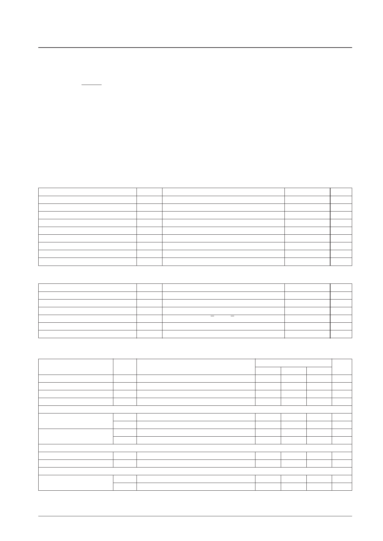
Specifications
Absolute Maximum Ratings at Tc = 25°C
Parameter
Maximum supply voltage1
Maximum supply voltage2
Input voltage
Phase output current
Repeatable avalanche current
Power loss
Operating substrate temperature
Junction temperature
Storage temperature
Symbol
VCC1 max
VCC2 max
VIN max
IOH max
Ear max
Pd max
Tc max
Tj max
Tstg
Conditions
No signal
No signal
Logic input pins
0.5 seconds, single pulse, with VCC1 applied.
θc-a = 0
Ratings
Unit
52
V
–0.3 to +7.0
V
–0.3 to +7.0
V
3.3
A
30
mJ
8
W
105
°C
150
°C
–40 to +125
°C
Allowable Operating Ranges at Ta = 25°C
Parameter
Supply voltage1
Supply voltage2
Input voltage
Phase driver voltage handling
Phase current 1
Phase current 2
Symbol
VCC1
VCC2
VIH
VDSS
IOH 1
IOH 2
Conditions
With input signals present
With input signals present
Tr1, 2, 3, and 4 (the A, A, B, and B outputs)
Tc = 105°C, CLK ≥ 200 Hz
Tc = 80°C, CLK ≥ 200 Hz
Ratings
Unit
10 to 45
V
5 ±5%
V
0 to VCC2
V
100 (min)
V
2.8
A
3
A
Electrical Characteristics at Tc = 25°C, VCC1 = 24 V, VCC2 = 5 V
Parameter
Control supply current
Output saturation voltage
Average output current
FET diode Forward voltage
[Control Inputs]
Input voltage
Input current
[Vref Input Pin]
Input voltage
Input current
[Control Outputs]
Output voltage
Symbol
Conditions
ICC
Vsat
Io ave
Vdf
Pin 6 input, with ENABLE pin held low.
RL = 12 Ω
Load: R = 3.5 W/L = 3.8 mH per phase
If = 1 A
VIH Except for the Vref pin
VIL Except for the Vref pin
IIH
Except for the Vref pin
IIL
Except for the Vref pin
VI
Pin 7
II
Pin 7, 2.5-V input
VOH I = –3 mA, pin MOI
VOL I = +3 mA, pin MOI
min
0.445
Ratings
typ
2.1
0.65
0.5
1
Unit
max
14 mA
1
V
0.56
A
1.5
V
4
V
1
V
0
1
10
µA
125
250
510
µA
0
2.5
V
330
415
545
µA
2.4
V
0.4
V
Continued on next page.
No. 6507-2/17
Share Link: