LS7560 查看數據表(PDF) - LSI Corporation
零件编号
产品描述 (功能)
生产厂家
LS7560 Datasheet PDF : 8 Pages
| |||
S2
S1
S3
VM
S1
S2
S3
VR
VM
24
S1
25
S2
26
S3
27
F/R
21 PWM CNTRL
20
TOP DRV
POL SEL
17
OUT1
16
OUT2
O U T 3 15
O U T 4 14
O U T 5 13
12
OUT6
22
BRAKE SEL
( + ) 10
23
OVERCURRENT
BRAKE
SENSE
11
(-)
1 SEQ SEL
TACH OUT 5
2
7
ENABLE
(-)
8
ERROR OUT
19
AMP
6
(+)
VR
18
V SS
28
V DD
9
OSC
3 FAULT
4
RC
**
* R2
100K
*R1
1.0M
* 10K
R3
CT
RT
CS Rs
ROTOR
* C1 * TYPICAL
0.1µF VALUES
VR
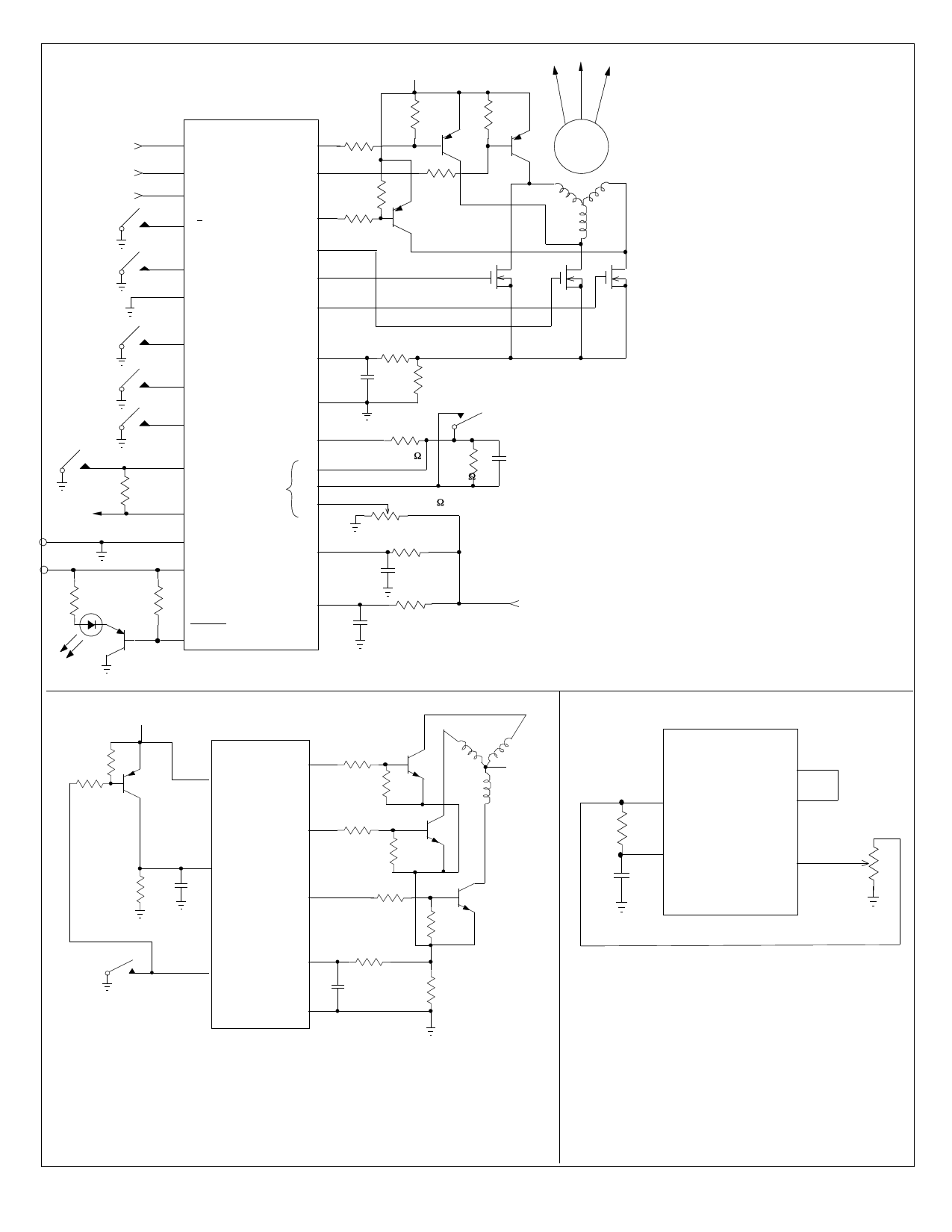
FIGURE 3. The closed loop mo-
tor control operation is achieved
by applying the Tachometer
Output at Pin 5 into the negative
terminal of the Error Amplifier
(Pin 7) through an R1-C1-R2 in-
tegrating network. The R1-C1
network is configured as a feed-
back circuit around the amplifier.
Since the Tachometer Output
has a fixed positive pulse width,
the average value of the pulse
train is directly proportional to
the motor speed. The desired
speed is selected by applying a
voltage at the positive input
(Pin 6) of the Error Amplifier.
The resultant output voltage of
the Error Amplifier is applied to
an internal Comparator along
with a ramp waveform gener-
ated by the RC Network at Pin
9. The PWM signal at the Com-
parator output is used to drive
outputs 1 thru 6 and complete
the closed loop. For this con-
figuration, Pin 20, the Top Driver
Polarity Select must be tied to
Ground.
FIGURE 3. THREE PHASE CLOSED LOOP FULL WAVE MOTOR CONTROLLER
VR
12
OUT6
19 V R
VM
13
OUT5
2
ENABLE
R
C
14
OUT4
ERROR AMP(-) 7
19 V R
8
ERROR AMP
OUT
RT
9 OSC
6
ERROR AMP(+)
CT
23
BRAKE
10
(+)
OVERCURRENT
S E N S E 11
(-)
FIGURE 4. THREE PHASE HALF WAVE MOTOR CONTROLLER
FIGURE 4. This three phase half wave motor controller has no top power tran-
sistor to disconnect the windings from the power supply when the BRAKE is ap-
plied. Instead, a switching transistor is used which will permit braking for a time
determined by the RC time constant. When the capacitor discharges past the
ENABLE input switching point, the outputs will be turned off.
7560-120497-5
FIGURE 5. OPEN LOOP CONTROLLER
FIGURE 5. In this configuration, the PWM output
duty cycle to the motor drivers is directly pro-
portional to the DC voltage applied to Pin 6, since
Pins 7 and 8 are tied together.
Share Link: 