MD82C288-10 查看數據表(PDF) - Intel
零件编号
产品描述 (功能)
生产厂家
MD82C288-10 Datasheet PDF : 20 Pages
| |||
M82C288
Symbol
INTA
VCC
GND
Type
O
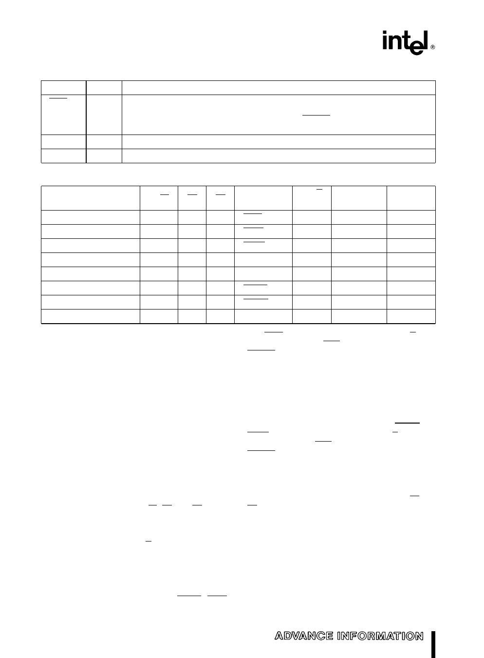
Table 1 Pin Description (Continued)
Name and Function
INTERRUPT ACKNOWLEDGE tells an interrupting device that its interrupt request
is being acknowledged This command output is active LOW The MB and CMDLY
inputs control when this output becomes active READY controls when it becomes
inactive
System Power a5V Power Supply
System Ground 0V
Table 2 Command and Control Outputs for Each Type of Bus Cycle
Type of
Bus Cycle
M IO
S1
S0
Command
Activated
DT R
State
ALE DEN
Issued
Interrupt Acknowledge
0
0
0
INTA
LOW
YES
I O Read
0
0
1
IORC
LOW
YES
I O Write
0
1
0
IOWC
HIGH
YES
None Idle
0
1
1
None
HIGH
NO
Halt Shutdown
1
0
0
None
HIGH
NO
Memory Read
1
0
1
MRDC
LOW
YES
Memory Write
1
1
0
MWTC
HIGH
YES
None Idle
1
1
1
None
HIGH
NO
MCE
Issued
YES
NO
NO
NO
NO
NO
NO
NO
Operating Modes
Two types of buses are supported by the M82C288
MULTIBUS I and non-MULTIBUS I When the MB
input is strapped HIGH MULTIBUS I timing is used
In MULTIBUS I mode the M82C288 delays com-
mand and data activation to meet IEEE-796 require-
ments on address to command active and write data
to command active setup timing MULTIBUS I mode
requires at least one wait state in the bus cycle since
the command outputs are delayed The non-
MULTIBUS I mode does not delay any outputs and
does not require wait states The MB input affects
the timing of the command and DEN outputs
and INTA) control outputs (ALE DEN DT R) and
control inputs (CEN AEN CENL CMDLY MB and
READY) are identical for all read bus cycles Read
cycles differ only in which command output is acti-
vated The MCE control output is only asserted dur-
ing interrupt acknowledge cycles
Write bus cycles activate different control and com-
mand outputs with different timing than read bus cy-
cles Memory write and I O write are write bus cy-
cles whose timing for command outputs (MWTC and
IOWC) control outputs (ALE DEN DT R) and con-
trol inputs (CEN AEN CENL CMDLY MB and
READY) are identical They differ only in which com-
mand output is activated
Command and Control Outputs
The type of bus cycle performed by the local bus
master is encoded in the M IO S1 and S0 inputs
Different command and control outputs are activat-
ed depending on the type of bus cycle Table 2 indi-
cates the cycle decode done by the M82C288 and
the effect on command DT R ALE DEN and MCE
outputs
Bus cycles come in three forms read write and
halt Read bus cycles include memory read I O
read and interrupt acknowledge The timing of the
associated read command outputs (MRDC IORC
Halt bus cycles are different because no command
or control output is activated All control inputs are
ignored until the next bus cycle is started via S1 and
S0
Static Operation
All M82C288 circuitry is of static design Internal reg-
isters and logic are static and require no refresh as
with dynamic circuit design This eliminates the mini-
mum operating frequency restriction placed on the
HMOS M82288 The CHMOS III M82C288 can oper-
ate from DC to the appropriate upper frequency limit
4
Share Link: 