T35L3232B 查看數據表(PDF) - Taiwan Memory Technology
零件编号
产品描述 (功能)
生产厂家
T35L3232B Datasheet PDF : 19 Pages
| |||
tm TE
CH
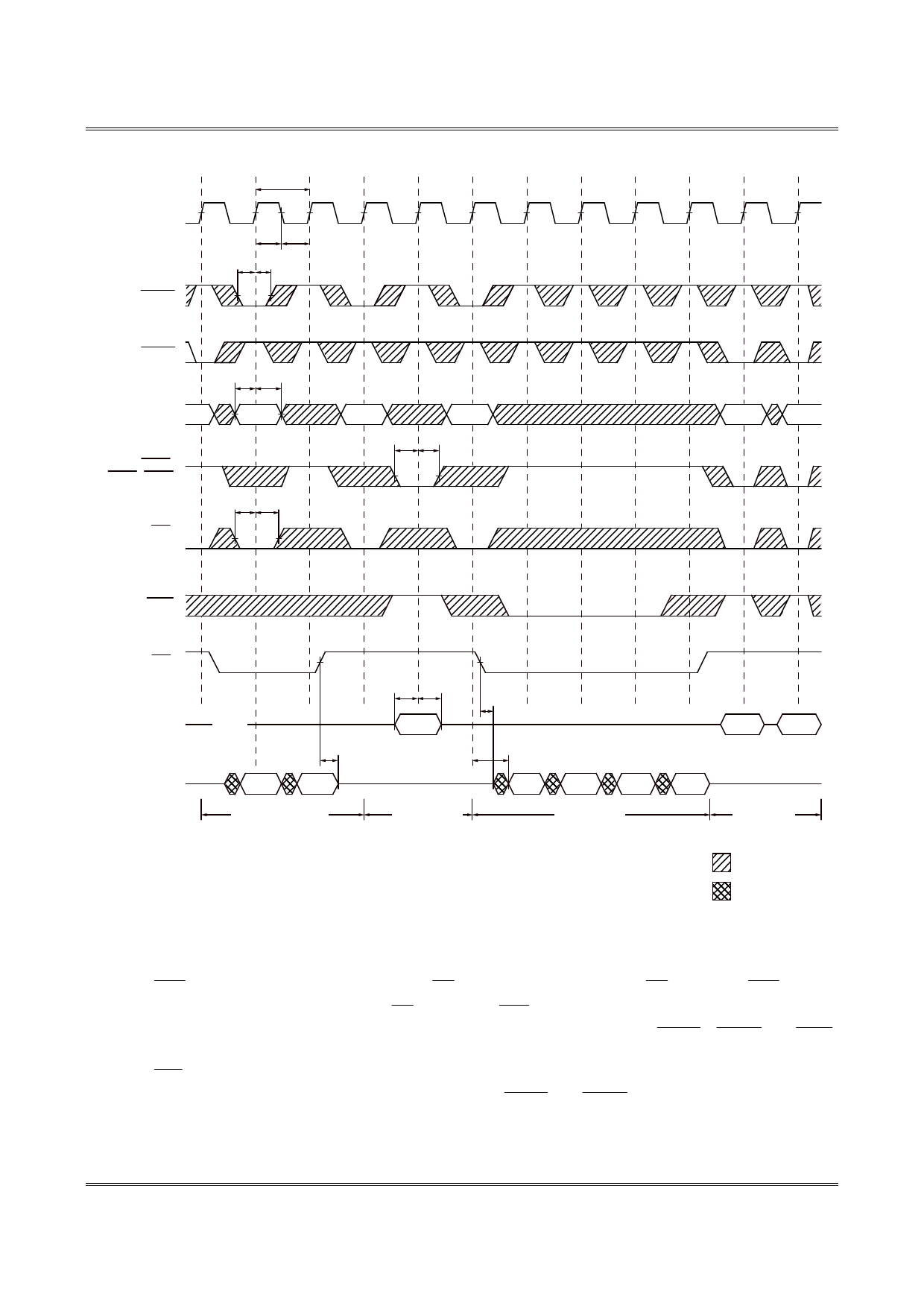
FLOW-THROUGH READ/WRITE TIMING
CLK
t KC
t KH t KL
t ADSS t ADSH
ADSP
Preliminary T35L3232B
AD S C
AD D RE S S A 1
t AS t AH
A2
BWE
BW1-BW4
(NOTE4)
CE
(NOTE2)
t CES t CEH
A3
A4
tWS tWH
A5
A6
ADV
OE
D
Q
High-Z
tOE HZ
Q(A1 )
Q(A2 )
Ba ck-to -B ac k R EADs
t DS t DH
D(A3)
Si ng le W R ITE
tOEL Z
t KQ
(NOTE1 )
Q(A4 )
Q(A4 +1)
Q (A4+2 )
BURST READ
D(A5)
D(A6)
Q(A4 +3)
Back-to -Ba ck
W R ITEs
DON'T CARE
UNDEFINED
Note: 1. Q(A4) refers to output from address A4. Q (A4 + 1) refers to output from the next internal burst
address following A4.
2. CE2 and CE2 have timing identical to CE . On this diagram, when CE is LOW, CE2 is
LOW and CE2 is HIGH. When CE is HIGH, CE2 is HIGH and CE2 is LOW.
3. The data bus (Q) remains in High-Z following a WRITE cycle unless an ADSP , ADSC or ADV
cycle is performed.
4. GW is HIGH.
5. Back-to-back READs may be controlled by either ADSP or ADSC.
Taiwan Memory Technology, Inc. reserves the right P. 16
to change products or specifications without notice.
Publication Date: FEB. 2000
Revision:0.A
Share Link: 