TA2009 查看數據表(PDF) - Toshiba
零件编号
产品描述 (功能)
生产厂家
TA2009 Datasheet PDF : 8 Pages
| |||
TA2009F/P
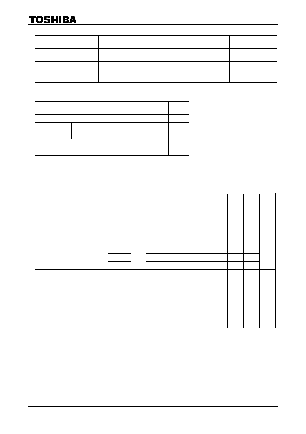
Pin
No.
Symbol
I/O
Function & Operation
14
RI
I R channel reverse input terminal.
15
RI
I R channel forward input terminal.
16
GND16
— Ground terminal for R channel reverse input side filter.
Remarks
Connect to RO of
TC9237BF, TC9237BN
Connect to RO of
TC9237BF, TC9237BN
—
Maximum Ratings (Ta = 25°C)
Characteristic
Symbol
Rating
Unit
Supply voltage
TA2009F
Power dissipation
TA2009P
Operating temperature
Storage temperature
VCC
PD
Topr
Tstg
11
V
350 (*)
mW
1388 (**)
-35~85
°C
-55~150
°C
(*) Reduce 2.8mW / °C at Ta = above 25°C.
(**) Reduce 11.2mW / °C at Ta = above 25°C.
Electrical Characteristics (unless otherwise specified, VCC = 5V, Ta = 25°C)
Characteristic
Operating supply
voltage
Symbol
VCC
Test
Cir-
Test Condition
cuit
— Ta = -35~85°C
Min. Typ.
4.5
5.0
Operating supply
current
Reference voltage
ICCQ (1)
ICCQ (2)
VRI
At no signal
—
At signal, VCC = 10V
—
—
7.5 10.0
8.2 11.0
2.45 2.50
Noise distortion factor
Cross talk
Attenuation
Max. output level
Differential balance
THD (1)
THD (2)
THD (3)
CT
ATT (1)
ATT (2)
Vomax
GVB
1kHz, Vo = 970mVrms
1 10kHz, Vo = 970mVrms
1kHz, Vo = 97mVrms
1 1kHz, Vo = 970mVrms
1 40kHz, Vo = 10dBVrms
80kHz, Vo = 10dBVrms
1 1kHz, THD = 1%
1
1kHz, 1.1dBVrms
In-phase input
—
-93
—
-93
—
-78
— -100
0.51 0.71
1.50 2.70
1.20 1.25
—
—
LR output difference
GVD
1
1kHz, 1.1dBVrms
Differential input
—
0
Max.
10
12.5
13.8
2.55
-90
-90
-75
-95
1.41
4.50
—
-40
0.5
Unit
V
mA
V
dB
dB
dB
Vrms
dB
dB
(Note 1) When the TC9237BF, C9237BN and +5V single power supply are operated
: Full scale = 970mVrms (typ.)
(Note 2) Measuring circuit-1: Indicates the measuring circuit.
3
2002-10-30
Share Link: 