HT9580 查看數據表(PDF) - Holtek Semiconductor
零件编号
产品描述 (功能)
生产厂家
HT9580 Datasheet PDF : 63 Pages
| |||
Preliminary
HT9580
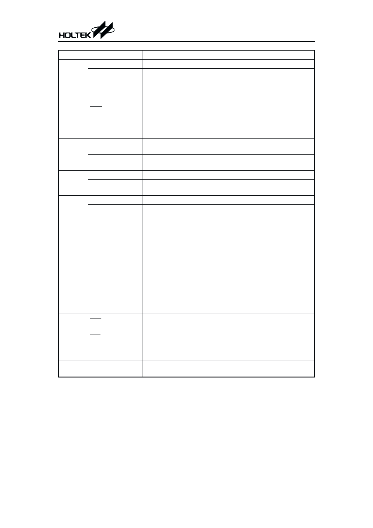
Pin No. Pin Name
BAL
58
SRDY
59
BAF
60
DA_OUT
61
RSSI
DI
62
MISO
BS3
63
MOSI
BS2
64
SCK
BS1
65
SS
66
TS
72~67 PA0~PA5
73
RESET
74
TSC
75
TS1
77
OSC1
76
OSC2
80
X1
79
X2
I/O
Description
I Battery voltage detector input with pull-high resistor.
SPI slave ready ¾ This slave ready pin is a Schmitt trigger input
with pull-high resistor. When the slave initiates the SPI transfer,
I a high to low transition activates an interrupt. When the master
initiates the SPI transfer, a high to low transition trigger the
master to start the transfer.
I Battery fail indication input, active low.
O D/A converter output. This pin is an 8-bit D/A analog output
I
RSSI output from IF circuit. This pin should be pulled high or low
externally when this pin is not used.
I
POCSAG code input serial data. CMOS input with pull-high re-
sistor.
I
SPI master-in-slave-out ¾ this is the data input with pull-high
resistor for SPI communications.
O PLL power control enable, CMOS output
O
SPI master-out-slave-in ¾ this is the data output for SPI commu-
nications.
O RF quick charge control enable, CMOS output
SPI serial clock ¾ the SCK signal is used to synchronize the data
I/O
transfer. If HT9580 is in the master mode, the SCK is output
clock. Otherwise, SCK is input clock if HT9580 is in the slave
mode.
O Pager receiver power control enable output, CMOS output
O
SPI slave select ¾ this signal is used to enable the SPI slave for
transfer.
I Decoder test mode input pin, active low with pull-high resistor.
General Input/Output Port A. These ports can be programmed to
have a wake-up capability for applications in keyboard operations
I/O or as normal I/O. Also the input cell structures are all Schmitt
trigger types and can be selected between CMOS or CMOS with
pull-high resistors.
I Schmitt trigger reset input, active low.
I
mC test mode input pin, active low with internal pull-high resis-
tor. The test circuit will be activated when this pin pulls low.
I
Decoder test mode input pin, active low with pull-high resistor.
The internal test mode will be activated when this pin pulls low.
I OSC1 and OSC2 are connected to an RC network to form a main
O clock oscillator
I X1 and X2 are connected to a crystal to form an internal low power
O clock oscillator (32.768kHz, 76.8kHz, or 153.6kHz)
5
April 28, 2000
Share Link: 