TC7126CPL 查看數據表(PDF) - Microchip Technology
零件编号
产品描述 (功能)
生产厂家
TC7126CPL Datasheet PDF : 26 Pages
| |||
1.0 ELECTRICAL
CHARACTERISTICS
Absolute Maximum Ratings*
Supply Voltage (V+ to V-)....................................... 15V
Analog Input Voltage (either Input) (Note 1) ... V+ to V-
Reference Input Voltage (either Input) ............ V+ to V-
Clock Input ................................................... Test to V+
Package Power Dissipation (TA ≤ 70°C) (Note 2):
44-Pin PQFP............................................... 1.00W
40-Pin PLCC ............................................... 1.23W
44-Pin PDIP ................................................ 1.23W
Operating Temperature Range:
C (Commercial) Devices .................. 0°C to +70°C
I (Industrial) Devices .................... -25°C to +85°C
Storage Temperature Range.............. -65°C to +150°C
TC7126/A
*Stresses above those listed under “Absolute
Maximum Ratings” may cause permanent damage to
the device. These are stress ratings only and functional
operation of the device at these or any other conditions
above those indicated in the operation sections of the
specifications is not implied. Exposure to Absolute
Maximum Rating conditions for extended periods may
affect device reliability.
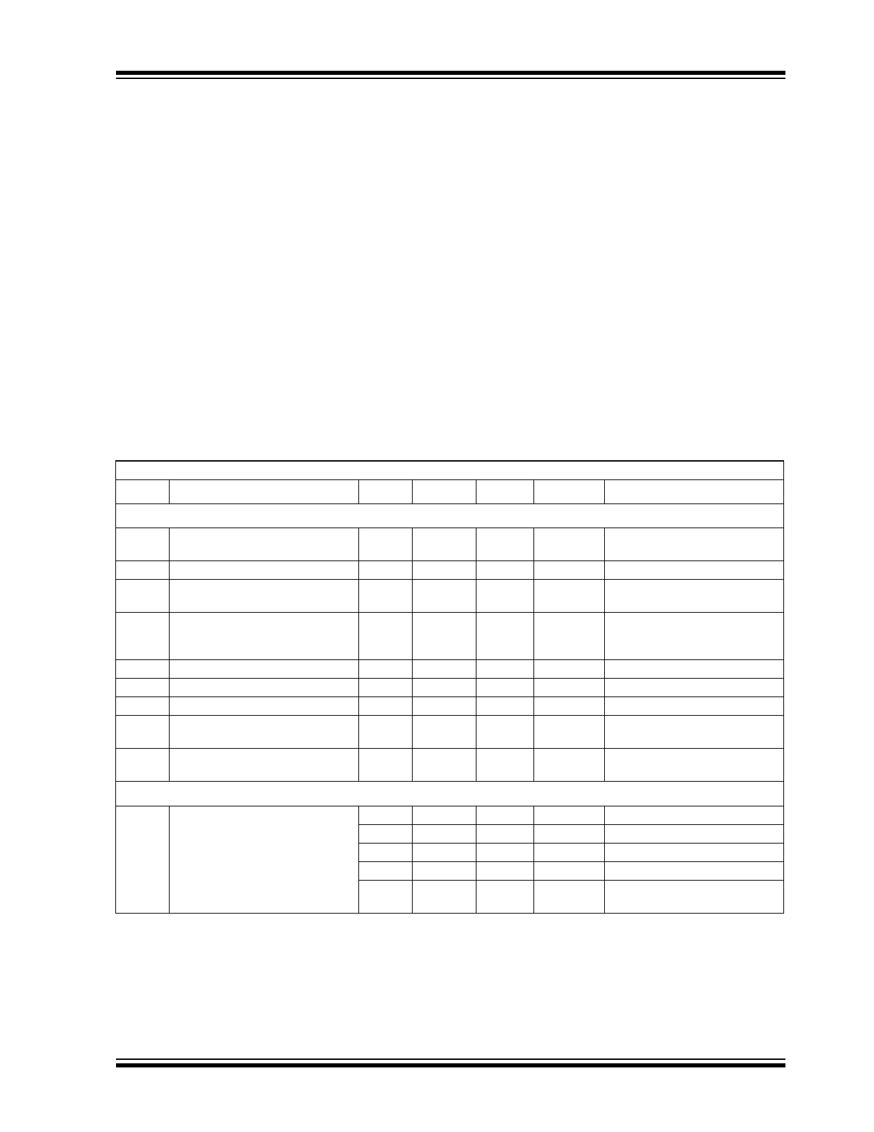
TABLE 1-1: TC7126/A ELECTRICAL SPECIFICATIONS
Electrical Characteristics: VS = +9V, fCLK – 16kHz, and TA = +25°C, unless otherwise noted.
Symbol
Parameter
Min
Typ
Max
Unit
Test Conditions
Input
ZIR
Zero Input Reading
ZRD
Zero Reading Drift
Ratiometric Reading
NL
Linearity Error
eN
IL
CMRR
Rollover Error
Noise
Input Leakage Current
Common Mode Rejection Ratio
Scale Factor Temperature
Coefficient
-000.0 ±000.0 +000.0
—
0.2
1
999 999/1000 1000
-1
±0.2
1
-1
±0.2
1
—
15
—
—
1
10
—
50
—
—
1
5
Digital
Reading
μV/°C
Digital
Reading
Count
Count
μVP-P
pA
μV/V
ppm/°C
VIN = 0V
Full Scale = 200mV
VIN = 0V, 0°C ≤ TA ≤ +70°C
VIN = VREF, VREF = 100mV
Full Scale = 200mV or 2V
Max Deviation From Best Fit
Straight Line
VIN- = VIN+ ≈ 200mV
VIN = 0V, Full Scale = 200mV
VIN = 0V
VCM = ±1V, VIN = 0V
Full Scale = 200mV
VIN = 199mV, 0°C ≤ TA ≤ +70°C
Ext. Ref. Temp Coeff. = 0ppm/°C
Analog Common
VCTC
Analog Common Temperature
Coefficient
—
—
—
—
—
80
—
—
250kΩ Between Common and V+
—
—
0°C ≤ TA ≤ +70°C (“C” Devices)
—
ppm/°C TC7126
—
35
75
ppm/°C TC7126A
—
35
100
ppm/°C -25°C ≤ TA ≤ +85°C (“I” Device)
(TC7126A)
Note 1: Input voltages may exceed the supply voltages, provided the input current is limited to ±100μA.
2: Dissipation rating assumes device is mounted with all leads soldered to printed circuit board.
3: Refer to “Differential Input” discussion.
4: Backplane drive is in phase with segment drive for “OFF” segment, 180° out of phase for “ON” segment. Frequency is
20 times conversion rate. Average DC component is less than 50mV.
5: See “Typical Application”.
6: During Auto-Zero phase, current is 10-20μA higher. A 48kHz ocillator increases current by 8μA (Typical). Common
current is not included.
© 2006 Microchip Technology Inc.
DS21458C-page 5
Share Link: 