TC7662A 查看數據表(PDF) - TelCom Semiconductor Inc => Microchip
零件编号
产品描述 (功能)
生产厂家
TC7662A Datasheet PDF : 5 Pages
| |||
CHARGE PUMP
DC-TO-DC CONVERTER
TC7662A
ABSOLUTE MAXIMUM RATINGS*
Supply Voltage VDD to GND .................................... +18V
Input Voltage (Any Pin) ........... (VDD + 0.3) to (V SS – 0.3)
Current Into Any Pin ................................................. 10mA
Operating Temperature Range
C Suffix .................................................. 0°C to +70°C
I Suffix .............................................. – 25°C to +85°C
E Suffix ............................................. – 40°C to +85°C
M Suffix .......................................... – 55°C to +125°C
Power Dissipation (TA ≤ 70°C)
Plastic DIP ......................................................730mW
CerDIP ............................................................ 800mW
Package Thermal Resistance
CPA, EPA θJA .............................................. 140°C/W
IJA, MJA θJA .................................................. 90°C/W
Storage Temperature Range ................ – 65°C to +150°C
Lead Temperature (Soldering, 10 sec) ................. +300°C
ESD Protection ..................................................... ±2000V
Output Short Circuit ................. Continuous (at 5.5V Input)
*Static-sensitive device. Unused devices must be stored in conductive
material. Protect devices from static discharge and static fields. Stresses
above those listed under Absolute Maximum Ratings may cause perma-
nent damage to the device. These are stress ratings only and functional
operation of the device at these or any other conditions above those
indicated in the operational sections of the specifications is not implied.
Exposure to Absolute Maximum Rating Conditions for extended periods
may affect device reliability.
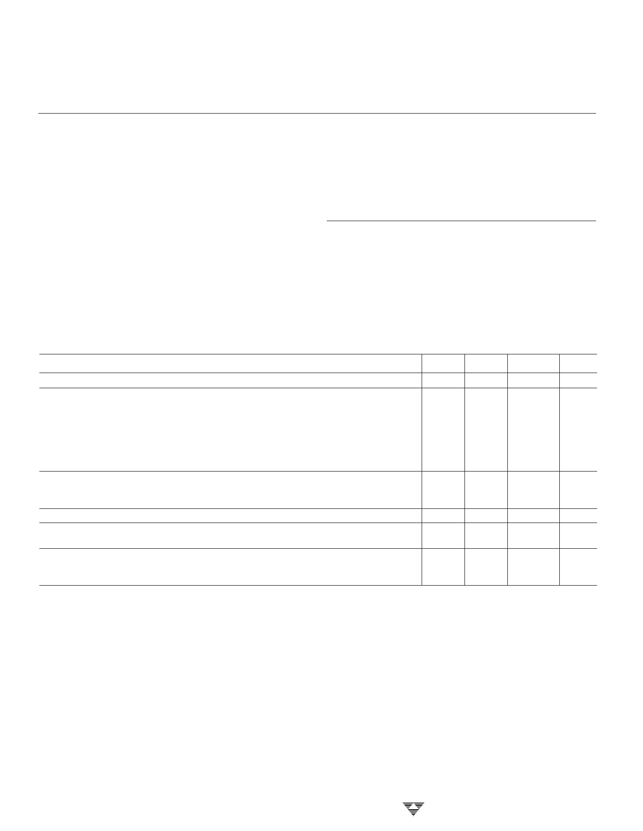
ELECTRICAL CHARACTERISTICS: VDD = 15V, TA = +25°C (See Test Circuit), unless otherwise specified.
Symbol
VDD
IS
Parameter
Supply Voltage
Supply Current
VDD = +15V
VDD = +5V
RO
COSC
PEFF
VEFF
Output Source
Resistance
Oscillator Frequency
Power Efficiency
Voltage Efficiency
Test Conditions
Min
3
RL = ∞
—
0°C ≤ TA ≤ +70°C
—
– 55°C ≤ TA ≤ +125°C
—
—
0°C ≤ TA ≤ +70°C
—
– 55°C ≤ TA ≤ +125°C
—
IL = 20mA, VDD = +15V
—
IL = 40mA, VDD = +15V
—
IL = 3mA, VDD = +5V
—
—
VDD = +15V
93
RL = 2 kΩ
VDD = +15V
99
RL = ∞
Over Operating Temperature Range
96
Typ Max
—
18
510
700
560
—
650
—
190
—
210
—
210
—
40
50
50
60
100
125
12
—
97
—
99.9
—
—
—
Unit
V
µA
Ω
kHz
%
%
4-78
TELCOM SEMICONDUCTOR, INC.
Share Link: 