TC7652 查看數據表(PDF) - Microchip Technology
零件编号
产品描述 (功能)
生产厂家
TC7652 Datasheet PDF : 16 Pages
| |||
TC7652
3.0 DETAILED DESCRIPTION
3.1 Capacitor Connection
Connect the null storage capacitors to the CA and CB
pins with a common connection to the CRET pin (14-pin
TC7652) or to VSS (8-pin TC7652). When connecting to
VSS, avoid injecting load current IR drops into the
capacitive circuitry by making this connection directly
via a separate wire or PC trace.
3.2 Output Clamp
In chopper stabilized amplifiers, the output clamp pin
reduces overload recovery time. When a connection is
made to the inverting input pin (summing junction), a
current path is created between that point and the out-
put pin, just before the device output saturates. This
prevents uncontrolled differential input voltages and
charge build-up on correction storage capacitors. Out-
put swing is reduced.
3.3 Clock
The TC7652 has a 550Hz internal oscillator, which is
divided by two before clocking the input chopper
switches. The 275Hz chopping frequency is available
at INT CLK OUT (Pin 12) on 14-pin devices. In normal
operation, INT/EXT (Pin 14), which has an internal pull-
up, can be left open.
An external clock can also be used. To disable the
internal clock and use an external one, the INT/EXT pin
must be tied to VSS. The external clock signal is then
applied to the EXT CLK IN input (Pin 13). An internal
divide-by-two provides a 50% switching duty cycle. The
capacitors are only charged when EXT CLK IN is high,
so a 50% to 80% positive duty cycle is recommended
for higher clock frequencies. The external clock can
swing between VDD and VSS, with the logic threshold
about 2.5V below VDD.
The output of the internal oscillator, before the divide-
by-two circuit, is available at EXT CLK IN when INT/
EXT is high or unconnected. This output can serve as
the clock input for a second TC7652 (operating in a
master/slave mode), so that both op amps will clock at
the same frequency. This prevents clock intermodula-
tion effects when two TC7652's are used in a differen-
tial amplifier configuration.
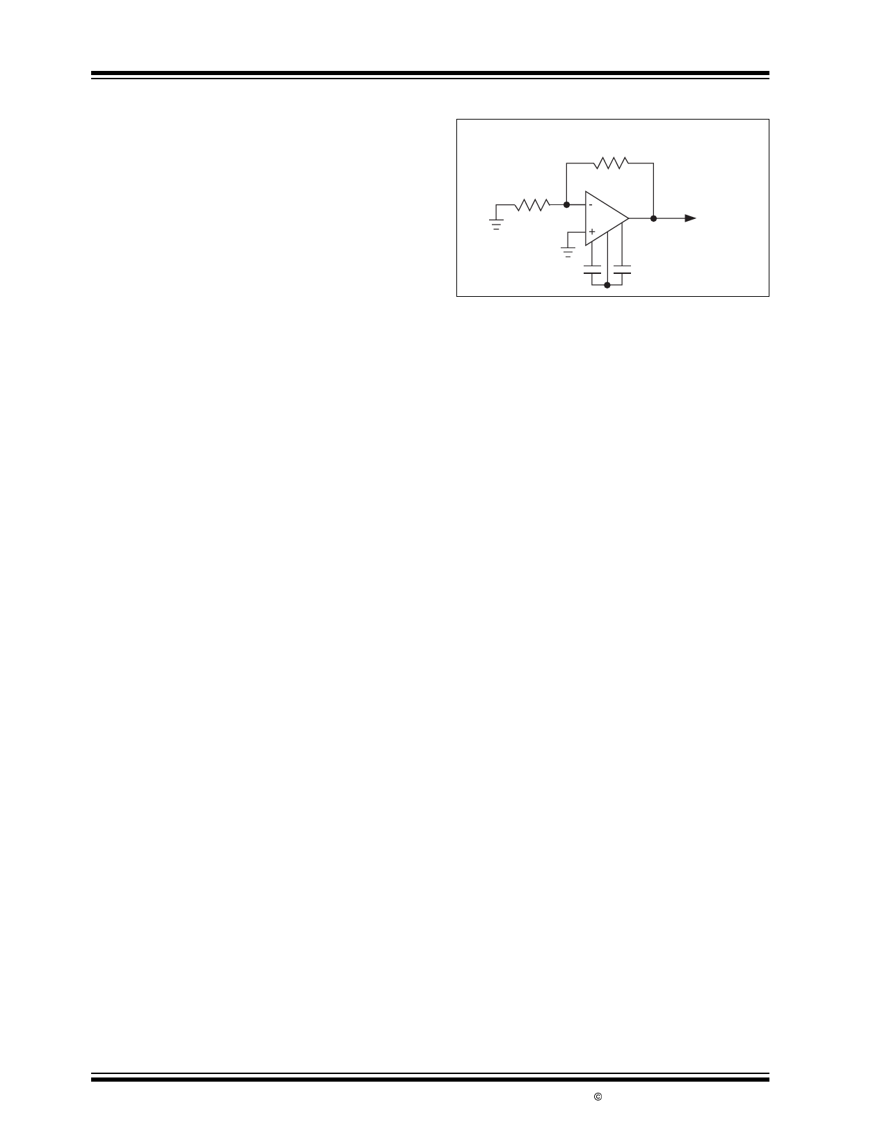
FIGURE 3-1:
TEST CIRCUIT
R2
1MΩ
R1
TC7652
1kΩ
-
+
C
R
C
0.1µF
0.1µF
Output
If the TC7652's output saturates, error voltages on the
external capacitors will slow overload recovery. This
condition can be avoided if a strobe signal is available.
The strobe signal is applied to EXT CLK IN and the
overload signal is applied to the amplifier while the
strobe is LOW. In this case, neither capacitor will be
charged. The low leakage of the capacitor pins allow
long measurements to be made within eligible errors
(typical capacitor drift is 10µV/sec).
4.0 TYPICAL APPLICATIONS
4.1 Component Selection
CA and CB (external capacitors)should be in the 0.1µF
to 1µF range. For minimum clock ripple noise, use a
1µF capacitor in broad bandwidth circuits. For limited
bandwidth applications where clock ripple is filtered
out, use a 0.1µF capacitor for slightly lower offset volt-
age. High quality, film type capacitors (polyester or
polypropylene) are recommended, although a lower
grade ceramic may work in some applications. For
quickest settling after initial turn-on, use low dielectric
absorption capacitors (e.g., polypropylene). With
ceramic capacitors, settling to 1µV takes several sec-
onds.
4.2 Static Protection
Although input diodes static protect all device pins,
avoid strong electrostatic fields and discharges that
can cause degraded diode junction characteristics and
produce increased input-leakage currents.
DS21464B-page 6
© 2002 Microchip Technology Inc.
Share Link: 