M80C186 查看數據表(PDF) - Intel
零件编号
产品描述 (功能)
生产厂家
M80C186 Datasheet PDF : 59 Pages
| |||
M80C186
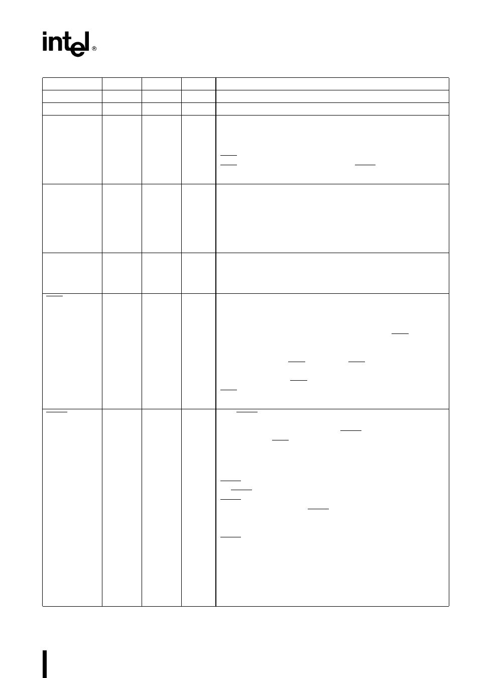
Symbol
VCC VCC
VSS VSS
RESET
X1 X2
CLKOUT
RES
TEST BUSY
PGA
9 43
26 60
57
59 58
56
24
47
Table 1 M80C186 Pin Description
QFP
1 35
52 18
21
19 20
22
54
31
Type
I
I
O
I
O
I
I
Name and Function
System Power a5 volt power supply
System Ground
Reset Output indicates that the M80C186 CPU is being
reset and can be used as a system reset It is active HIGH
synchronized with the processor clock and lasts an integer
number of clock periods corresponding to the length of the
RES signal Reset goes inactive 2 clockout periods after
RES goes inactive When tied to the TEST BUSY pin Reset
forces the M80C186 into enhanced mode
Crystal Inputs X1 and X2 provide external connections for a
fundamental mode or third overtone parallel resonant crystal
for the internal oscillator X1 can connect to an external
clock instead of a crystal In this case minimize the
capacitance on X2 or drive X2 with complemented X1 The
input or oscillator frequency is internally divided by two to
generate the clock signal (CLKOUT)
Clock Output provides the system with a 50% duty cycle
waveform All device pin timings are specified relative to
CLKOUT CLKOUT has sufficient MOS drive capabilities for
the Numeric Processor Extension
System Reset causes the M80C186 to immediately
terminate its present activity clear the internal logic and
enter a dormant state This signal may be asynchronous to
the M80C186 clock The M80C186 begins fetching
instructions approximately 7 clock cycles after RES is
returned HIGH For proper initialization VCC must be within
specifications and the clock signal must be stable for more
than 4 clocks with RES held LOW RES is internally
synchronized This input is provided with a Schmitt-trigger to
facilitate power-on RES generation via an RC network When
RES occurs the M80C186 will drive the status lines to an
inactive level for one clock and then float them
The TEST pin is sampled during and after reset to determine
whether the M80C186 is to enter Compatible or Enhanced
Mode Enhanced Mode requires TEST to be HIGH on the
rising edge of RES and LOW four clocks later Any other
combination will place the M80C186 in Compatible Mode A
weak internal pullup insures a HIGH state when the pin is not
driven
TEST In Compatible Mode this pin is configured to operate
as TEST This pin is examined by the WAIT instruction If the
TEST input is HIGH when WAIT execution begins instruction
execution will suspend TEST will be resampled every five
clocks until it goes LOW at which time execution will resume
If interrupts are enabled while the M80C186 is waiting for
TEST interrupts will be serviced
BUSY In Enhanced Mode this pin is configured to operate
as BUSY The BUSY input is used to notify the M80C186 of
Numerics Processor Extension activity Floating point
instructions executing in the M80C186 sample the BUSY pin
to determine when the Numerics Processor is ready to
accept a new command BUSY is active HIGH
3
Share Link: 