TDA3562 查看數據表(PDF) - STMicroelectronics
零件编号
产品描述 (功能)
生产厂家
TDA3562 Datasheet PDF : 9 Pages
| |||
TDA3562A
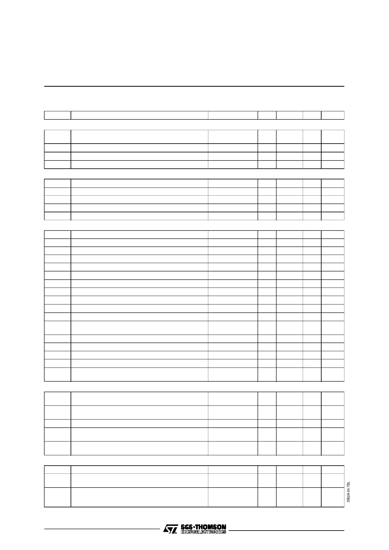
ELECTRICAL CHARACTERISTICS (continued)
Symbol
Parameter
Test Conditions
”BLACK CURRENT” STABILIZATI ON INPUT (pin 18) (continued)
Difference between Input Voltage for ”BlackCurrent”
and Leakage Current
Input Resistance during Scan
Input Current during ”Black Current” Measurement
Input Current during Scan
RGB - OUTPUTS (Pins 13, 15, 17)
Output Resistance
Current Source
Peak Output Level
Residual 4.4 MHz at RGB Outputs
Residual 8.8 MHz at RGB Outputs
LUMINANCE CHANNEL
Frequency Resp. of Total Lumin. Amplifiers
RGB Output Signal (black to white)
Relative Spread of RGB - Output Signals
f = 0 to 5MHz
Contrast Control Range
Tracking Over 10 dB Contrast Control
Contrast Control Input Current
(see fig. 1)
Blanking Level of RGB - Output Signals
Difference Between Blanking Levels,
Differential Drift of Blanking Levels
Brightness Control Input Current
∆T = 40 °C
Brightness Control Range
Relation Ship between Black Level Variation and
Brightness Control Variation
Black Level of RGB Output Signals
Difference between Black Levels
Tracking Over Brightness Control
Differential Drift of Black Levels
Drift of Black Level Versus 10 % Variation of Supply
Voltage and Contrast Control
(see fig. 3)
(see fig. 3)
(see note 4)
(see note 4)
∆T = 40 °C
”CUT OFF CURRENT” REGULATION
RGB Output Level of the ”3L Windows” after Switch-
on
RGB Outputs Level of the ”3L Windows” after Cut
off Current Stabilization
RGB Output Range
Charge/Discharge Current during Measuring Time
(3L windows) at Pins 10, 19, 20 and 21
Leakage Currents Flowing into Pins 10, 20 and 21
during Scan
(see note 4)
RGB DATA INSERTION
Data RGB Output Signal
Differential Amplitude Error between RGB Output
Signal and Data Output Signal
Differential Error between Black Levels of RGB
Output Signals and Black Levels of Data Output
Signals
V9 = 0.9 to 3V
Min.
2
10.7
3.5
0
7.5
1
1
Typ. Max.
0.5
1.5
2
10
50
3
11.3
100
150
–1
–3
4
4.5
1
–5 to 10
0
15
1
1.2
mV
0
5
1 to 3
1.3
3
0
2
20
20
3
5
5
1
50
4
10
200
Unit
V
kΩ
µA
mA
Ω
mA
V
mVpp
mVpp
dB
Vpp
dB
dB
dB
µA
V
mV
µA
V
V/V
V
mV
%
mV
mV
V
V
V
mA
nA
Vpp
%
mV
4/9
Share Link: 