TDA7269SA 查看數據表(PDF) - STMicroelectronics
零件编号
产品描述 (功能)
生产厂家
TDA7269SA Datasheet PDF : 11 Pages
| |||
TDA7269SA
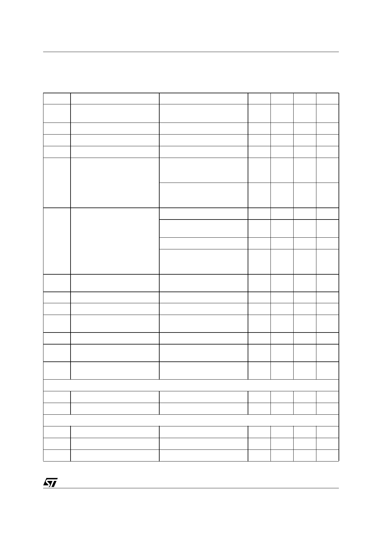
Table 4. ELECTRICAL CHARACTERISTCS
(Refer to the test circuit VS = ±14V; RL = 8Ω; RS = 50Ω; GV = 30dB, f = 1KHz; Tamb = 25°C, unless otherwise
specified)
Symbol
Parameter
Test Condition
Min. Typ. Max. Unit
VS Supply Voltage Range
RL = 8Ω;
RL = 4Ω;
±5
±20
V
±5
±15
V
Iq
Total Quiescent Current
VOS Input Offset Voltage
60
100 mA
-25
25
mV
Ib
PO
THD
Non Inverting Input Bias Current
Output Power
Total Harmonic Distortion
THD = 10%;
RL = 8Ω;
VS = ±12.5V; RL = 4Ω;
THD = 1%;
RL = 8Ω;
VS = ±12.5V; RL = 4Ω;
RL = 8Ω; PO = 1W; f = 1KHz;
RL = 8Ω; PO = 0.1 to 5W;
f = 100Hz to 15KHz;
500
nA
8
10
W
7.5
10
W
7.5
W
7.5
W
0.03
%
0.7
%
RL = 4Ω; PO = 1W; f = 1KHz;
RL = 4Ω; VS = ±10V;
PO = 0.1 to 5W;
f = 100Hz to 15KHz;
0.02
%
1
%
CT Cross Talk
f = 1KHz;
f = 10KHz;
70
dB
50
60
dB
SR Slew Rate
6.5
10
V/µs
GOL Open Loop Voltage Gain
eN Total Output Noise
Ri
SVR
Input Resistance
Supply Voltage Rejection
(each channel)
A Curve
f = 20Hz to 22KHz
f = 100Hz; VR = 0.5V
80
3
4
15
20
60
dB
µV
8
µV
KΩ
dB
Tj
Thermal Shut-down Junction
Temperature
145
°C
MUTE FUNCTION [ref +VS] (*)
VMUTE Mute /Play threshold
AMUTE Mute Attenuation
STAND-BY FUNCTIONS [ref: +VS] (only for Split Supply)
VST-BY Stand-by Mute threshold
AST-BY Stand-by Attenuation
IqST-BY Quiescent Current @ Stand-by
(*) In mute condition the current drawn from Pin 5 must be ≤650µA
-7
-6
-5
V
60
70
dB
-3.5 -2.5 -1.5
V
110
dB
3
6
mA
3/11
Share Link: 