TEA1507 查看數據表(PDF) - Philips Electronics
零件编号
产品描述 (功能)
生产厂家
TEA1507 Datasheet PDF : 20 Pages
| |||
Philips Semiconductors
GreenChip™II SMPS control IC
Preliminary specification
TEA1507
Current mode control
Current mode control is used for its good line regulation
behaviour.
The ‘on-time’ is controlled by the internally inverted control
pin voltage, which is compared with the primary current
information. The primary current is sensed across an
external resistor. The driver output is latched in the logic,
preventing multiple switch-on.
The internal control voltage is inversely proportional to the
external control pin voltage, with an offset of 1.5 V. This
means that a voltage range from 1 to 1.5 V on pin CTRL
will result in an internal control voltage range from
0.5 to 0 V (the maximum external control voltage results in
a minimum duty cycle).
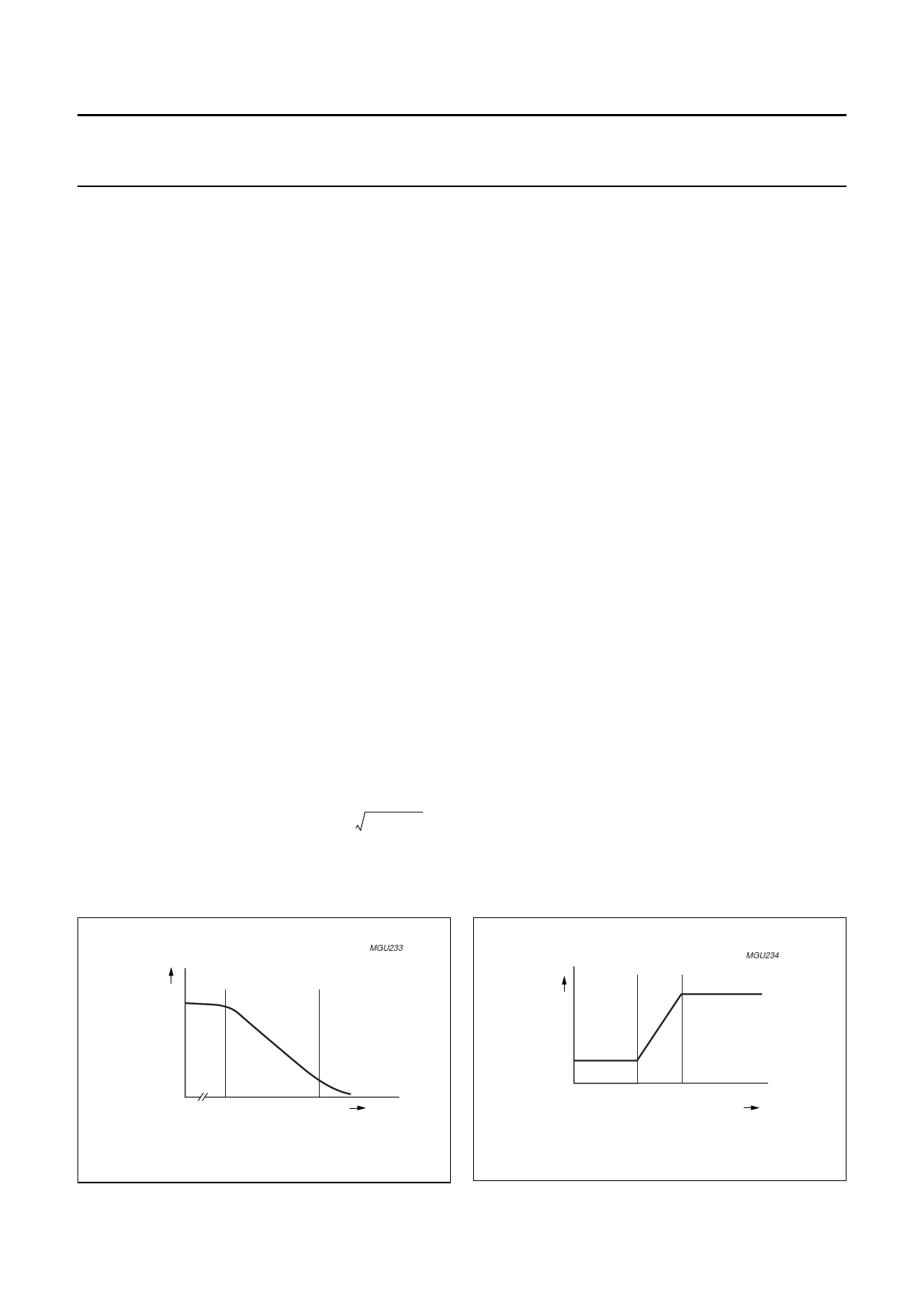
Oscillator
The maximum fixed frequency of the oscillator is set by an
internal current source and capacitor. The maximum
frequency is reduced once the control voltage enters the
VCO control window. Then, the maximum frequency
changes linearly with the control voltage until the minimum
frequency is reached (see Figs 5 and 6).
Valley switching (see Fig.7)
A new cycle starts when the power switch is switched on.
After the ‘on-time’ (which is determined by the ‘sense’
voltage and the internal control voltage), the switch is
opened and the secondary stroke starts. After the
secondary stroke, the drain voltage shows an oscillation
with a frequency of approximately -------------------------1--------------------------
(2 × π × (Lp × Cd))
where Lp is the primary self inductance of the transformer
and Cd is the capacitance on the drain node.
As soon as the oscillator voltage is high again and the
secondary stroke has ended, the circuit waits for the
lowest drain voltage before starting a new primary stroke.
This method is called valley detection. Figure 7 shows the
drain voltage together with the valley signal, the signal
indicating the secondary stroke and the oscillator signal.
In an optimum design, the reflected secondary voltage on
the primary side will force the drain voltage to zero. Thus,
zero voltage switching is very possible, preventing large
capacitive switching losses P = 12-- × C × V2 × f , and
allowing high frequency operation, which results in small
and cost effective inductors.
Demagnetization
The system will be in discontinuous conduction mode all
the time. The oscillator will not start a new primary stroke
until the secondary stroke has ended.
Demagnetization features a cycle-by-cycle output
short-circuit protection by immediately lowering the
frequency (longer off-time), thereby reducing the power
level.
Demagnetization recognition is suppressed during the first
tsuppr time. This suppression may be necessary in
applications where the transformer has a large leakage
inductance and at low output voltages/start-up.
Minimum and maximum ‘on-time’
The minimum ‘on-time’ of the SMPS is determined by the
Leading Edge Blanking (LEB) time. The IC limits the
‘on-time’ to 50 µs. When the system desires an ‘on-time’
longer than 50 µs, a fault condition is assumed (e.g.
removed Ci), the IC will stop switching and enter the safe
restart mode.
handbook, halVfpsaegnese(max)
0.5 V
MGU233
handbook, halfpage f
MGU234
175 kHz
1V
(typ)
1.5 V
(typ)
VCTRL
Fig.5 The Vsense(max) voltage as function of VCTRL.
6 kHz
50 mV 75 mV Vsense(max)
(typ) (typ)
Fig.6 The VCO frequency as function of Vsense(max)
2000 Dec 05
6
Share Link: 