TK73211 查看數據表(PDF) - Toko America Inc
零件编号
产品描述 (功能)
生产厂家
TK73211 Datasheet PDF : 16 Pages
| |||
TK732xx
DEFINITION AND EXPLANATION OF TECHNICAL TERMS
OUTPUT VOLTAGE (VOUT)
The output voltage is specified with VIN = (VOUT(TYP) + 1 V)
and IOUT = 30 mA.
DROPOUT VOLTAGE (VDROP)
The dropout voltage is the difference between the input
voltage and the output voltage at which point the regulator
starts to fall out of regulation. Below this value, the output
voltage will fall as the input voltage is reduced. It is
dependent upon the load current, the external transistor
and the junction temperature.
BASE CONTROL CURRENT (IBASE)
The base control current is the drive current for the base of
the external transistor.
OUTPUT CURRENT (IOUT)
The output current depends on the characteristics of the
external transistor and current limit setting.
LINE REGULATION (Line Reg)
RIPPLE REJECTION RATIO (RR)
Ripple rejection is the ability of the regulator to attenuate
the ripple content of the input voltage at the output. It is
specified with 100 mVrms, 400 Hz superimposed on the
input voltage, where VIN = VOUT(TYP) + 1.5 V. The output
decoupling capacitor is set to 10 µF, the noise bypass
capacitor is set to 0.1 µF, and the load current is set to
30 mA. Ripple rejection is the ratio of the ripple content of
the output vs. the input and is expressed in dB.
STANDBY CURRENT (ISTBY)
Standby current is the current which flows into the regulator
when the output is turned off by the control function
(VCONT = 0 V). It is measured with VIN = 8 V (9 V for the
8 V output device).
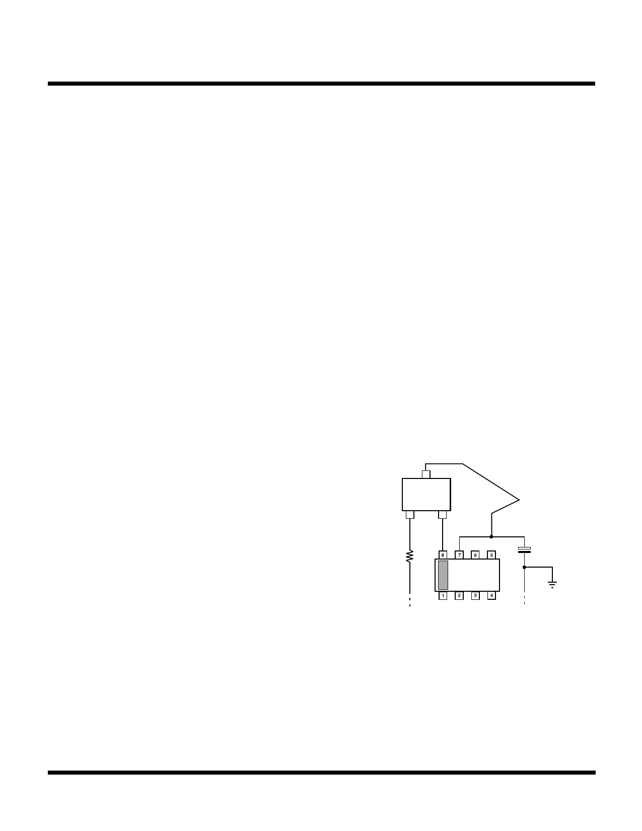
REMOTE SENSING (VSENSE)
The VSENSE pin is the output voltage sensing pin. If the
voltage drop to the load caused by the PCB etch resistance
cannot be disregarded, the voltage drop can be
compensated by connecting the VSENSE pin as shown
below.
Line regulation is the ability of the regulator to maintain a
constant output voltage as the input voltage changes. The
line regulation is specified as the input voltage is changed
from VIN = VOUT(TYP) + 1 V to VIN = VOUT(TYP) + 6 V.
LOAD REGULATION (Load Reg)
COLLECTOR
EXTERNAL
TRANSISTOR
EMITTER
BASE
VOUT
Load regulation is the ability of the regulator to maintain a
constant output voltage as the load current changes. It is
a pulsed measurement to minimize temperature effects.
Load regulation depends on the external transistor.
RIPK
CL
TK732XX
QUIESCENT CURRENT (IQ)
The quiescent current is the current which flows through
the ground terminal under no load conditions (IOUT = 0 mA)
and excludes the control pin current.
The length of the VSENSE etch should be limited to 30 cm
(11.8 in.) maximum.
GROUND CURRENT (IGND)
Ground current is the current which flows through the
ground pin(s). It is defined as IIN - IOUT, excluding control
current.
January 1999 TOKO, Inc.
Page 9
Share Link: 