TN0604WG 查看數據表(PDF) - Supertex Inc
零件编号
产品描述 (功能)
生产厂家
TN0604WG Datasheet PDF : 4 Pages
| |||
Thermal Characteristics
TN0602/TN0604
Package
TO-92
ID (continuous)*
1.0A
ID (pulsed)
4.6A
Power Dissipation
@ TC = 25°C
1W
SOW-20
Refer to Arrays & Special Functions Section.
* I (continuous) is limited by max rated T .
D
j
θjc
°C/W
125
θja
°C/W
170
IDR*
1.0A
IDRM
4.6A
Electrical Characteristics (@ 25°C unless otherwise specified)
Symbol
Parameter
Min Typ Max Unit
BVDSS Drain-to-Source
TN0604
40
V
Breakdown Voltage
TN0602
20
VGS(th)
∆VGS(th)
IGSS
IDSS
Gate Threshold Voltage
Change in VGS(th) with Temperature
Gate Body Leakage
Zero Gate Voltage Drain Current
0.6
-3.8
1.6
V
-4.5 mV/°C
100
nA
10
µA
1.0
mA
ID(ON)
ON-State Drain Current
RDS(ON)
Static Drain-to-Source TO-92/SOW-20
ON-State Resistance
TO-92
1.5 2.1
4.0 7.0
1.0
1.6
0.6 0.75
SOW - 20
1.0
∆RDS(ON) Change in RDS(ON) with Temperature
0.5 0.75
GFS
Forward Transconductance
0.5 0.8
CISS
Input Capacitance
140 190
COSS
Common Source Output Capacitance
75
110
CRSS
Reverse Transfer Capacitance
25
50
td(ON)
Turn-ON Delay Time
10
tr
Rise Time
6.0
td(OFF)
Turn-OFF Delay Time
25
tf
Fall Time
20
VSD
Diode Forward Voltage Drop
1.2
1.8
trr
Reverse Recovery Time
300
Notes:
1: All D.C. parameters 100% tested at 25°C unless otherwise stated. (Pulse test: 300µs pulse, 2% duty cycle.)
2: All A.C. parameters sample tested.
A
Ω
Ω
%/°C
pF
ns
V
ns
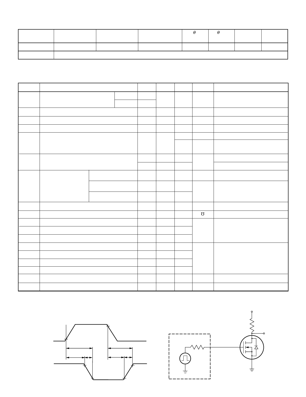
Switching Waveforms and Test Circuit
10V
INPUT
90%
0V 10%
t(ON)
t(OFF)
td(ON)
tr
td(OFF)
tF
VDD
OUTPUT
0V
10%
90%
10%
90%
7-48
PULSE
GENERATOR
Rgen
INPUT
Conditions
VGS = 0V, ID = 2.0mA
VGS = VDS, ID = 1.0mA
VGS = VDS, ID = 2.5mA
VGS = ±20V, VDS = 0V
VGS = 0V, VDS = Max Rating
VGS = 0V, VDS = 0.8 Max Rating
TA = 125°C
VGS = 5V, VDS = 20V
VGS = 10V, VDS = 20V
VGS = 5V, ID = 0.75A
VGS = 10V, ID = 1.5A
VGS = 10V, ID = 1.5A
VDS = 20V, ID = 1.5A
VGS = 0V, VDS = 20V
f = 1 MHz
VDD = 20V
ID = 0.5A
RGEN = 25Ω
VGS = 0V, ISD = 1.5A
VGS = 0V, ISD = 1A
VDD
RL
OUTPUT
D.U.T.
Share Link: 