AD7242(RevB) 查看數據表(PDF) - Analog Devices
零件编号
产品描述 (功能)
生产厂家
AD7242 Datasheet PDF : 12 Pages
| |||
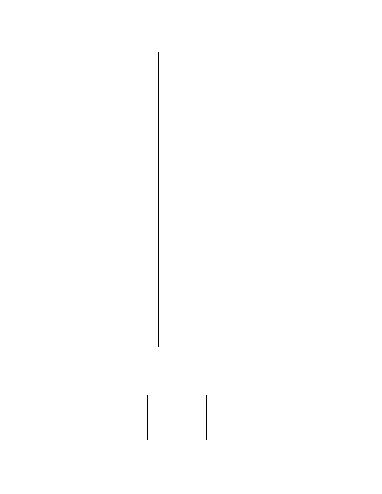
AD7242
Parameter
AD7244
J, A Versions1 S Version1
Units
Test Conditions/Comments
DC ACCURACY
Resolution
14
14
Integral Nonlinearity
±2
±2
Differential Nonlinearity
±1
±1
Bipolar Zero Error
± 10
± 10
Positive Full-Scale Error2
± 10
± 10
Negative Full-Scale Error2
± 10
± 10
Bits
LSB max
LSB max
LSB max
LSB max
LSB max
Guaranteed Monotonic
REFERENCE OUTPUT3
REF OUT @ +25°C
2.99/3.01
2.99/3.01
V min/V max
TMIN to TMAX
2.98/3.02
2.98/3.02
V min/V max
REF OUT Tempco
35
35
ppm/°C typ
Reference Load Change
(ΔREF OUT vs. ΔI)
–1
–1
mV max
Reference Load Current Change (0 μA–500 μA)
REFERENCE INPUTS
REF INA, REF INB Input Range
Input Current
E LOGIC INPUTS
(LDACA, LDACB, TFSA, TFSB,
TCLKA, TCLKB, DTA, DTB)
T Input High Voltage, VINH
Input Low Voltage, VINL
Input Current, IIN
Input Capacitance, CIN4
E ANALOG OUTPUTS
(VOUTA, VOUTB)
Output Voltage Range
DC Output Impedance
L Short Circuit Current
2.85/3.15
1
2.4
0.8
± 10
10
±3
0.1
20
2.85/3.15
1
2.4
0.8
± 10
10
±3
0.1
20
V min/V max 3 V ± 5%
μA max
V min
V max
μA max
pF max
V nom
Ω typ
mA typ
VDD = 5 V ± 5%
VDD = 5 V ± 5%
VIN = 0 V to VDD
AC CHARACTERISTICS4
Voltage Output Settling Time
Positive Full-Scale Change
4
4
O Negative Full-Scale Change
4
4
Digital-to-Analog Glitch Impulse 10
10
Digital Feedthrough
2
2
Channel-to-Channel Isolation
110
110
S POWER REQUIREMENTS
VDD
+5
+5
VSS
–5
–5
IDD
27
28
B ISS
15
15
Total Power Dissipation
195
205
μs max
μs max
nV secs typ
nV secs typ
dB typ
Settling Time to Within ± 1/2 LSB of Final Value
Typically 2.5 μs
Typically 2.5 μs
DAC Code Change All 1s to All 0s
VOUT = 10 kHz Sine Wave
V nom
V nom
mA max
mA max
mW max
± 5% for Specified Performance
± 5% for Specified Performance
Cumulative Current from the Two VDD Pins
Cumulative Current from the Two VSS Pins
Typically 130 mW
NOTES
1Temperature ranges are as follows: J Version: 0°C to +70°C; A Version: –40°C to +85°C; S Version: –55°C to +125°C.
O 2Measured with respect to REF IN and includes bipolar offset error.
3For capacitive loads greater than 50 pF, a series resistor is required (see Internal Reference section).
4Sample tested @ +25°C to ensure compliance.
Specifications subject to change without notice.
AD7244 ORDERING GUIDE
Model1
Temperature
Range
Integral
Nonlinearity
Package
Option2
AD7244JN
AD7244JR
AD7244AQ
AD7244SQ3
–40°C to +85°C
–40°C to +85°C
–40°C to +85°C
–55°C to +125°C
± 2 LSB max
± 2 LSB max
± 2 LSB max
± 2 LSB max
N-24
R-28
Q-24
Q-24
NOTES
1To order MIL-STD-883, Class B, processed parts, add /883B to part number.
Contact local sales office for military data sheet and availability.
2N = Plastic DIP; Q = Cerdip; R = Small Outline IC (SOIC).
3This grade will be available to /883B processing only.
REV. B
–3–
Share Link: 