AD7226 查看數據表(PDF) - Analog Devices
零件编号
产品描述 (功能)
生产厂家
AD7226 Datasheet PDF : 16 Pages
| |||

AD7226
CIRCUIT INFORMATION
D/A SECTION
The AD7226 contains four identical, 8-bit, voltage mode digital-to-
analog converters. The output voltages from the converters have the
same polarity as the reference voltage allowing single supply opera-
tion. A novel DAC switch pair arrangement on the AD7226 allows a
reference voltage range from 2 V to 12.5 V.
Each DAC consists of a highly stable, thin-film, R-2R ladder
and eight high speed NMOS, single-pole, double-throw
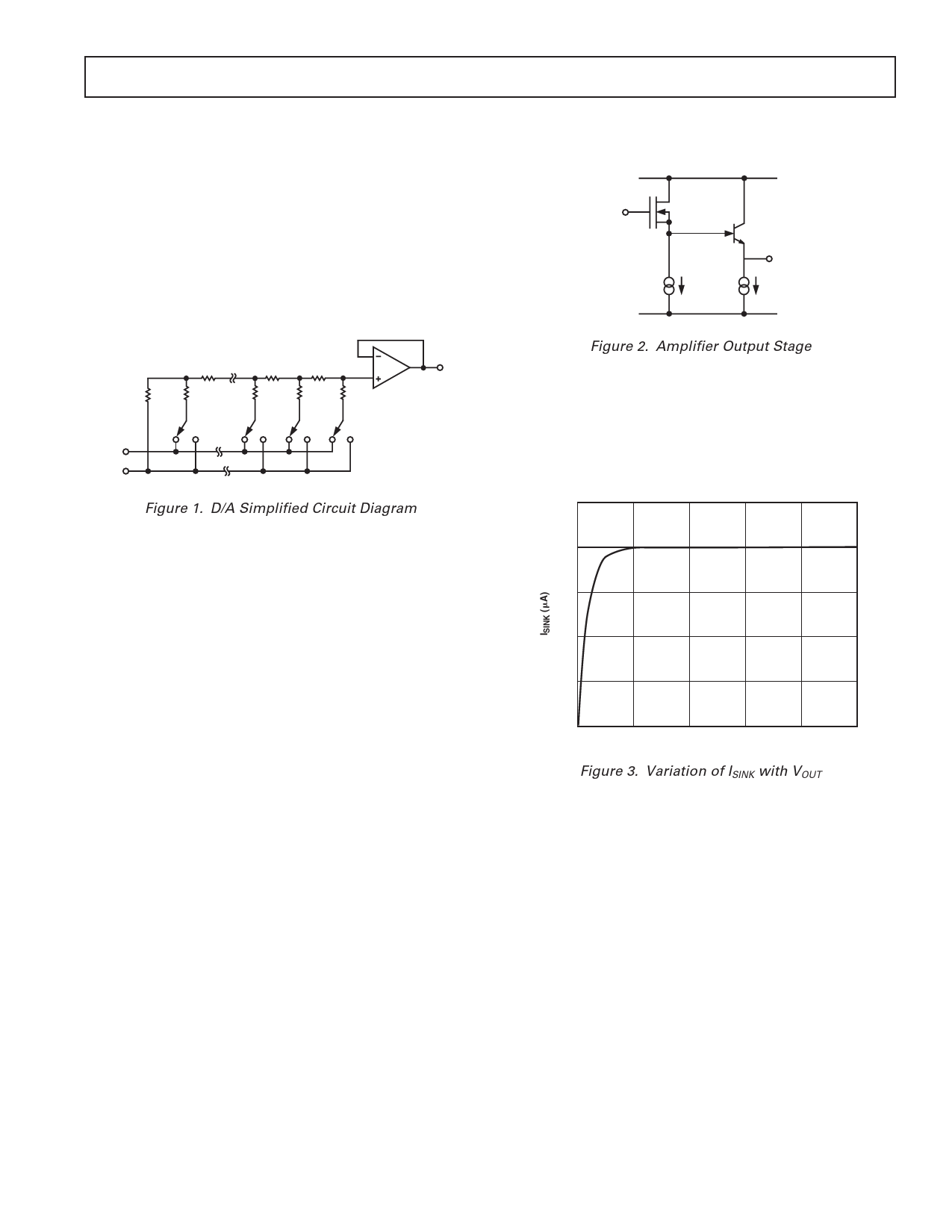
switches. The simplified circuit diagram for one channel is
shown in Figure 1. Note that VREF (Pin 4) and AGND (Pin 5)
are common to all four DACs.
R
2R
2R
DB0
R
2R
DB5
R
2R
2R
DB6
DB7
VOUT
VREF
AGND
SHOWN FOR ALL 1s ON DAC
Figure 1. D/A Simplified Circuit Diagram
The input impedance at the VREF pin of the AD7226 is the
parallel combination of the four individual DAC reference input
impedances. It is code dependent and can vary from 2 kW to
infinity. The lowest input impedance (i.e., 2 KW) occurs when
all four DACs are loaded with the digital code 01010101.
Therefore, it is important that the reference presents a low
output impedance under changing load conditions. The nodal
capacitance at the reference terminals is also code dependent
and typically varies from 100 pF to 250 pF.
Each VOUT pin can be considered as a digitally programmable
voltage source with an output voltage of:
VOUTX = DX VREF
(1)
where DX is fractional representation of the digital input code
and can vary from 0 to 255/256.
The source impedance is the output resistance of the buffer
amplifier.
OP AMP SECTION
Each voltage-mode D/A converter output is buffered by a unity
gain, noninverting CMOS amplifier. This buffer amplifier is
capable of developing 10 V across a 2 kW load and can drive
capacitive loads of 3300 pF. The output stage of this amplifier
consists of a bipolar transistor from the VDD line and a current
load to the VSS, the negative supply for the output amplifiers.
This output stage is shown in Figure 2.
The NPN transistor supplies the required output current drive
(up to 5 mA). The current load consists of NMOS transistors
which normally act as a constant current sink of 400 mA to VSS,
giving each output a current sink capability of approximately
400 mA if required.
The AD7226 can be operated single or dual supply resulting
in different performance in some parameters from the output
amplifiers.
In single supply operation (VSS = 0 V = AGND), with the out-
put approaching AGND (i.e., digital code approaching all 0s)
VDD
I/P
O/P
400A
VSS
Figure 2. Amplifier Output Stage
the current load ceases to act as a current sink and begins to act
as a resistive load of approximately 2 kW to AGND. This occurs
as the NMOS transistors come out of saturation. This means
that, in single supply operation, the sink capability of the ampli-
fiers is reduced when the output voltage is at or near AGND. A
typical plot of the variation of current sink capability with out-
put voltage is shown in Figure 3.
500
VSS = –5V
400
300
VSS = 0
200
VDD = +15V
100
0
0
2
4
6
8
10
VOUT (V)
Figure 3. Variation of ISINK with VOUT
If the full sink capability is required with output voltages at or
near AGND (= 0 V), then VSS can be brought below 0 V by 5 V
and thereby maintain the 400 mA current sink as indicated in
Figure 3. Biasing VSS below 0 V also gives additional headroom
in the output amplifier which allows for better zero code error
performance on each output. Also improved is the slew rate and
negative-going settling time of the amplifiers (discussed later).
Each amplifier offset is laser trimmed during manufacture to
eliminate any requirement for offset nulling.
DIGITAL SECTION
The digital inputs of the AD7226 are both TTL and CMOS
(5 V) compatible from VDD = 11.4 V to 16.5 V. All logic inputs
are static protected MOS gates with typical input currents of
less than 1 nA. Internal input protection is achieved by an
on-chip distributed diode from DGND to each MOS gate. To
minimize power supply currents, it is recommended that the
digital input voltages be driven as close to the supply rails (VDD
and DGND) as practically possible.
REV. D
–5–